3. Legacy PCI and PCI Express
Important
This article covers the PCI and PCIe buses. You can read about the specific AXI PCIe MM IP here.
3.1. Peripheral Component Interconnect
If you ever have built or looked inside a desktop, you may have noticed that a few boards connected to the motherboard all use the same interface. Since the 1990’s, computers have utilized the Peripheral Component Interconnect or PCI bus to attach additional components and hardware devices via expansion slots. Modern examples include graphics processing unit (GPU) boards and enthusiast-grade sound cards.
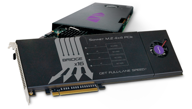
An example PCIe expansion card with x16 width
The PCI format allowed computer manufacturers to build and sell peripherals with a standardized format that was compatible with all motherboards and independent of any processor’s requirements, essentially creating a plug-and-play system. The legacy PCI bus and its upgraded version PCI-X were eventually made obsolete by their successor PCI Express, which we currently use in 2021.
Although many PCI peripherals are now integrated into the motherboard itself or available as external USB devices, the PCI bus remains relevant today due to its widespread usage among industrial and enthusiast fields. Since PCIe is backwards compatible with its older standards and builds upon PCI concepts, we will first examine the fundamentals of the legacy PCI standard.
3.2. PCI Overview and Background
As a component bus (a bus is essentially communication between multiple components), all PCI concepts revolve around maintaining and processing transactions between peripherals and the processor (CPU). The PCI bus can be thought of as a traffic light, controlling the flow of data transactions between devices while other peripherals must wait for their turn to use the PCI bus. The external PCI bus works in tandem with the system bus, which allows internal computer components like the CPU or RAM to communicate with each other, and other external buses like the Universal Serial Bus, such as connecting a printer using an external USB cable.
Legacy PCI is synchronous, in that all events occur on the edge of the computer’s internal clock. A device would begin a data transaction and specify a start memory address, taking one clock cycle. Sending the data itself would take multiple cycles until the transaction finished, at which point the connection was ended.
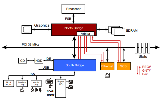
Abstraction of a computer’s core architecture
The PCI bus operates on a master-slave relationship, where the Bus Master is the agent that initiates the transaction (either the CPU or PCI boards) and the slave is the Target Device. Many modern devices have Bus Mastering capabilities, so an example transaction could involve a keyboard acting as a Bus Master to write data into main memory (the Target Device). This relationship can be further elaborated upon by looking at a motherboard’s core architecture.
The northbridge or host bridge represents the core logic chip on the PC’s motherboard that is ‘north’ of the central PCI bus. The northbridge interfaces between the CPU, system memory, the AGP (graphics) bus, and high-speed PCI bus. The northbridge’s Bus Arbiter receives requests from all initiators (Bus Masters), decides which requester should monopolize the PCI bus, creates the transaction channel between the initiator and Target Device, and assigns a ready pin (GNT#).
The southbridge serves as the I/O controller hub, hosting all system I/O and connecting the PCI bus to external peripherals. It also provides system signals like reset, clock, and error reporting. From the southbridge, Bus Masters representing a peripheral can submit a request to use and monopolize the PCI bus. Each Bus Master has a pair of pins that they can request with (REQ#) or know when the bus is available to use (GNT#).
3.3. The Legacy PCI Bus Cycle
As mentioned before, Legacy PCI is synchronous as in events occur on clock edges. To illustrate this bus cycle better, we will examine a simple example of a typical bus transaction. Rising clock edges are marked with dotted lines whenever signals are driven or sampled.
Note
Signals with # are active LOW, signals without are active HIGH.
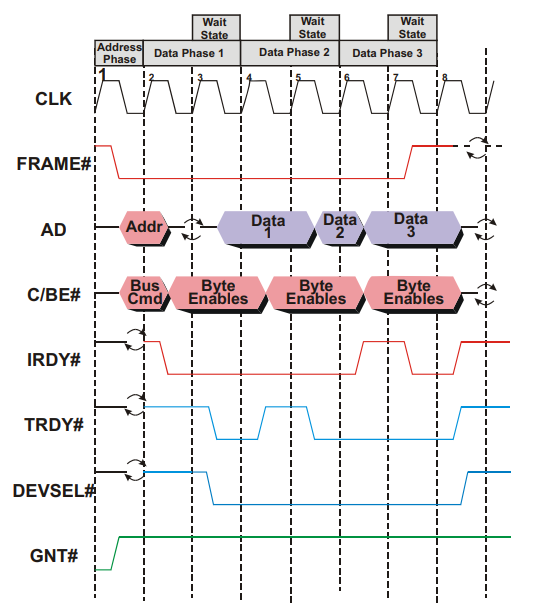
Example Legacy PCI bus cycle
CLK Edge 1 - FRAME# (Bus Access) and IRDY# (Initiator Ready for data) are inactive, so PCI bus is idle.
GNT# is active, showing that bus arbiter has selected this device to be the next initiator / Bus Master
CLK Edge 2 - FRAME# is asserted by the initiator, indicating that a new transaction has started.
Initiator drives address and command for the transaction, other devices on bus will decode address to determine if they are being requested
CLK Edge 3 - Initiator indicates that it is ready for data transfer by asserting IRDY# to active low
Arrow on AD bus shows that bus is undergoing turn-around cycle as ownership of signals changes (initiator drives address but also reads data on same pins)
TRDY# is not driven low on the same edge as AD changing to avoid possibility of both buffers trying to drive a signal simultaneously, which can cause damage from shared signals
CLK Edge 4 - Device on bus has recognized requested address and has asserted DEVSEL# (device select) to proceed with transaction
Also asserts TRDY# (target ready) to drive first part of read data onto AD bus
Since both IRDY# and TRDY# are active at the same time, data begins transferring on that clock edge
Initiator knows how many bytes will eventually be transferred, but target does not, so the target must check FRAME# to see if it is still asserted or not (will become inactive when done)
CLK Edge 5 - Target is not ready to deliver next set, so it de-asserts TRDY# for one clock cycle and enters a Wait State
CLK Edge 6 - Second data item is transferred, and since FRAME# is still asserted, the target knows that the initiator is still requesting for more data
CLK Edge 7 - Initiator forces a Wait State, allowing device to pause a transaction and either quickly fill or empty a buffer without stopping the request
Often very inefficient as they will both stall their current transaction and prevent bus access to other devices
CLK Edge 8 - Third data set is transferred, FRAME# is de-asserted so transaction is finished, at CLK edge 9 all control lines are turned off and bus becomes idle again