4. DDR Memory and SDRAM
4.1. What is RAM?
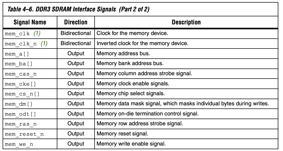
Inside any computer, phone, tablet, or other electronic device, it is almost guaranteed that there will be some sort of RAM inside that device. In fact, if you have ever looked inside a PC computer before, then you have most likely seen what a physical piece of RAM looks like. Below is an example of a DDR3 SDRAM component, and these can be purchased at most electronics stores (see Figure 1). The DDR stands for “Double-Data Rate’’, and the SDRAM stands for “Synchronous Dynamic RAM”. These are just terms used to describe the process of how the RAM stores data, and they will be explained in more detail further down.
Figure 1: Example DDR3 SDRAM Component
RAM stands for “Random-Access Memory”, and like all memories, it’s main purpose is to store information for future use. In your computer, for example, you should be able to check how much RAM is currently installed by going to your device settings. The more RAM that your computer has, the faster that it will be able to load programs and applications.
Almost all RAM components are “volatile” memory devices, which means that any stored data will be lost once the RAM loses power. Because of this, RAM is often used to store temporary data, such as program or application data. For more permanent storage of information, another type of memory such as “Read-Only Memory” (ROM) can be used instead. A good example of ROM is a CD disk, which is initially programmed with data (music, video, games, etc.) and is not meant to be overwritten (see Figure 2).

Figure 2: Example of CD ROM
Most computers have both RAM and ROM components inside them, as RAM is needed for storing program/application data and ROM is needed for storing permanent instructions (i.e: boot-up instructions). They both have their own advantages and disadvantages, and so there is always a tradeoff between speed and volatility. While RAM components are generally much faster than ROM components, ROM has the ability to retain information even after power has been removed from the device.
4.2. Different Types of RAM
RAM can come in all shapes and sizes, but the two most common types of RAM are “Static RAM (SRAM)” and “Dynamic RAM (DRAM)”. While both SRAM and DRAM are effective at storing temporary data, the main difference between them lies in how each of them store this data. SRAM is referred to as “static” because it is made up solely of transistors. DRAM, on the other hand, uses capacitors to store the data. Both have their own advantages and disadvantages, and so let’s take a closer look at each type of RAM.
4.3. SRAM
Looking at the figure below (figure 3), we can see what a typical SRAM cell configuration looks like. The parts labeled M1 through M6 are MOSFET transistors, the line labeled WL corresponds to the “Write Line”, and the line labeled BL corresponds to the “Bit Line”. The write line and the bit line are used simultaneously to control the read and write operations of the SRAM. For example, if we wanted to write a new bit value into this SRAM cell, we would simply place the desired bit value on the bit line (1 or 0), and then we would place a 1 on the write line to enable the write transaction.
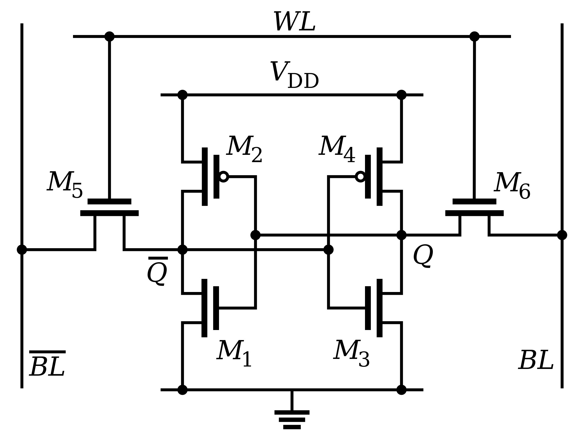
Figure 3: Typical SRAM Cell Configuration
The primary advantage of using SRAM components is that they are much faster than DRAM components. However, with the advantage of being faster, they are also much more expensive to manufacture. Therefore, SRAMs are typically only used for small amounts of memory that really need that extra speed. For example, a standard use of SRAM is for your computer’s cache memory, which stores frequently-used instructions and data for faster fetching by the CPU. Have you ever noticed that after you restart your computer, it takes slightly longer to load any given website? This is because your computer has information stored inside its cache that allows the website to load faster, and when you restart your computer, you are also clearing that cache memory.
4.4. DRAM
In comparison to SRAM components, DRAM utilizes capacitors in order to store memory. The typical configuration of a DRAM cell can be seen below in figure 4, and as you can see, the configuration appears to be much simpler than the SRAM cell. The bitline and the worldline are still present, and they are utilized in the same way as the SRAM cell. However, there are not nearly as many transistors required for the DRAM cell, which means that the cost to manufacture a DRAM component is far less than that of an SRAM component.
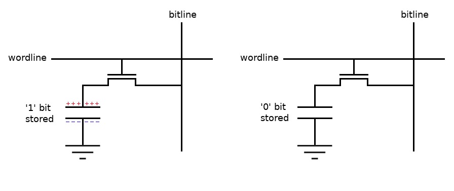
Figure 4: Typical DRAM Cell Configuration
The fact that DRAM components are much cheaper than SRAM components make them a great choice for storing large amounts of data. For example, when you purchase a large piece of RAM like the illustration in figure 1, you are purchasing DRAM (the term “SDRAM” refers to Synchronous DRAM). While SRAM components like cache memory are typically in the kilobyte to low megabyte range, DRAM components can go all the way up to gigabyte range. The primary disadvantage of DRAM is that it is usually slower than SRAM, and this is due to the effects of using a capacitor. Over time, capacitors can begin to slowly discharge, and this can be very bad if it causes the stored data to be lost. In order to prevent this, DRAM components have to be constantly “refreshed”, which essentially just means that the current data values have to be re-written into the capacitors.
4.5. The DDR SDRAM Protocol
If you look back to our example in figure 1, you’ll notice the specific memory part is called “DDR3 SDRAM”. Well, now that we know what DRAM is, let’s take a look at the rest of this name. First, let’s look at the term “SDRAM”. While this name may look similar to the Static RAM (SRAM) discussed earlier, it is actually referring to something very different. In a typical DRAM cell, there is no clock associated with the read and write transactions. However, digital electronics engineers are very fond of using clocks to keep everything synchronous in their designs, and so Synchronous DRAM (SDRAM) was created. This essentially means that read and write operations will only be processed on the rising edge of an associated clock.
Now that the read and write operations have been synchronized, a lot of the messiness has been cleaned up that could potentially occur from doing multiple asynchronous transactions. However, only sending data on one edge of a clock is rather slow, and it wastes time that could potentially be used for processing other transactions. Therefore, the Double Data Rate (DDR) protocol was created, and this process allows data to be sent on both the positive and the negative edge of an associated clock. This process can be seen below in figure 5.
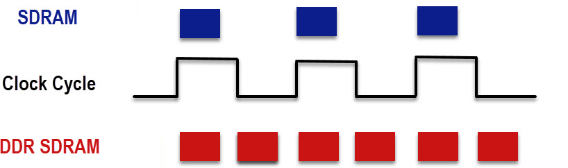
Figure 5: DDR SDRAM vs SDRAM Protocols
There have been many variations of the DDR SDRAM protocol, and the term “DDR3” refers to the third generation of this protocol. At this current time in 2021, DDR5 is the most current and up-to-date DDR protocol, and it was released in July of 2020. However, DDR3 and DDR4 are both still used widely in electronics today.
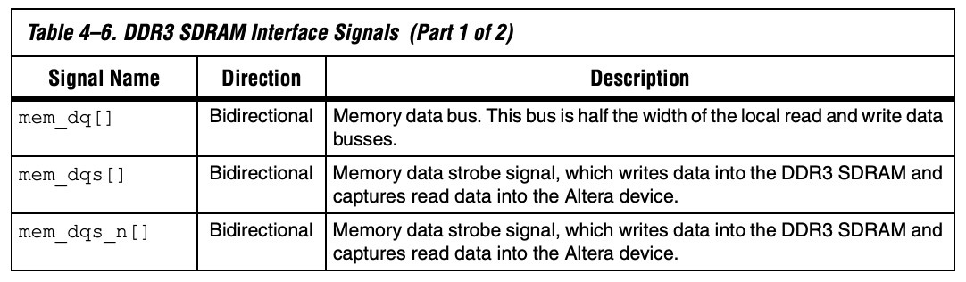
Specific information about timing, signals, resets, and more can all be found in the DDR3 SDRAM High-Performance Controller User Guide from Intel. For example, let’s take a look at this DDR3 Timing Diagram seen below in figure 6.
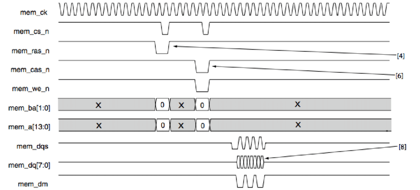
Figure 6: DDR3 Timing Diagram
At the top of this diagram is the memory clock, which is what the DDR memory device uses to clock its transactions. Then, right below the clock are the memory chip select signal, the row-address strobe signal, the column-address strobe signal, and the write enable signal. All four of these signals are used to set up or initialize the desired read or write transaction. After these signals come the memory bank bus and the memory address bus, and these point specifically to the memory location that you would like to read or write from. Finally, the memory strobe signal indicates when the data is being transferred, the data bus contains the specific data, and the memory data mask signal indicates which bytes of data should actually be transferred. For a greater description of these signals, see the attached “Table 4-6 DDR3 SDRAM Interface Signals” from the DDR3 SDRAM High-Performance Controller User Guide.