3. DMA/Bridge for PCIe IP Overview
3.1. DMA IP Overview
Xilinx’s DMA/Bridge Subsystem for PCI Express IP is an alternative to the AXI Memory Mapped to PCI Express IP, which was used previously in the “AXI Memory Mapped to PCI Express” section. It still provides a customizable PCIe interface to the FPGA, but this IP also utilizes the DMA (Direct Memory Access) protocol.
Xilinx’s user guide for this IP can be found here and Xilinx also provides an XDMA driver that can be used to interface with this IP over Windows 10 or Linux OS. This particular driver can be found here, and a helpful guide to using this driver can be found here. Essentially, instead of manually performing read and write operations to specific addresses (this is called Programmable Input/Output or PIO), DMA provides a much more efficient way to handle data transactions. The DMA PCIE IP core also provides an AXILite interface and an AXI Memory Mapped “Bypass” interface for simple PIO operations.
3.2. The DMA Protocol
The entire goal of DMA is to make data transactions more efficient and less work for the CPU. Instead of having to specify each transaction with the corresponding data and address, DMA allows for transfer of large batches of data, all independent of the CPU. In general, the DMA protocol works like this:
User specifies whether the transaction will be a “Host to Card” (H2C) or “Card to Host”. Data moving from the host machine to the FPGA will be considered H2C in this case.
User specifies the starting source address and starting destination address of the data, as well as the size of the transfer in bytes. If the transaction is H2C, then the source address will be in PCIe memory space and the destination address will be in AXI memory space.
The CPU programs the DMA engine with this information, and then the DMA begins transferring all of the data. Once the data has finished transferring, the DMA will send an interrupt back to the CPU.
This specific type of DMA engine is known as a “Scatter Gather” DMA, which means that the target data, source address, destination address, and transfer length are all configured in registers known as “Descriptors”. Each descriptor is stored in host memory, and they act as pointers to designated buffers within host memory based on the source/destination address and the transfer length specified. Here is an image from the Xilinx XDMA Driver Debugging Guide, which shows the exact configuration of the Descriptor registers:
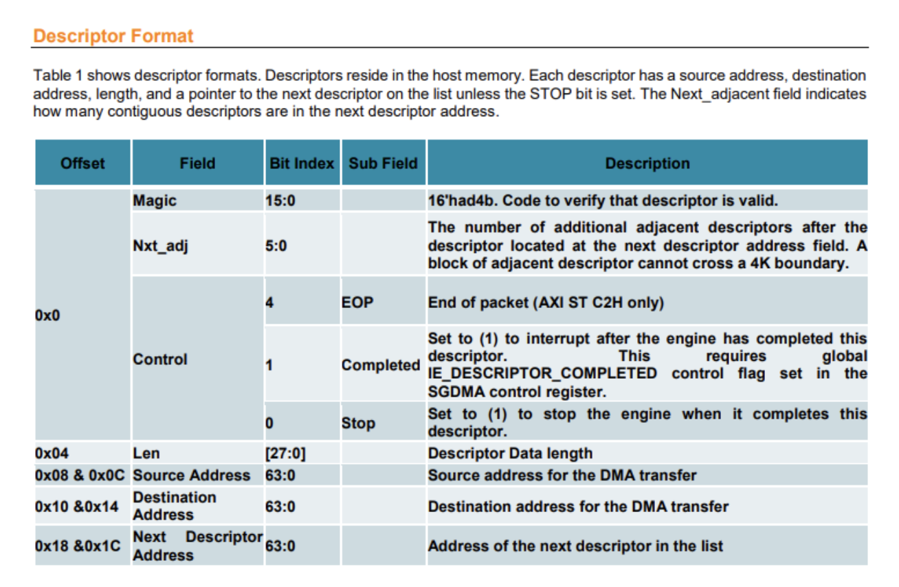
Figure 1: Xilinx DMA Descriptor Format
Once a descriptor register has been filled out with the correct information, then it is ready to perform the data transaction. In order to start the transaction, the user will need to write to a DMA control register (register 0x04 specifically) in order to enable the transaction. When the data is finished transmitting, the DMA will send an interrupt to the CPU, acknowledging the end of the transfer. More information about the DMA control registers can be found in Xilinx’s User Guide for the DMA PCIe IP.
Below is an image from the “DMA for PCI Express” Youtube video from Xilinx, which outlines the DMA process using the Descriptor registers. Each of the descriptors correspond to an allocated buffer within System Memory, and then that buffer is either filled by data from the FPGA (C2H transfer), or the data from that buffer is transferred to the FPGA (H2C transfer).
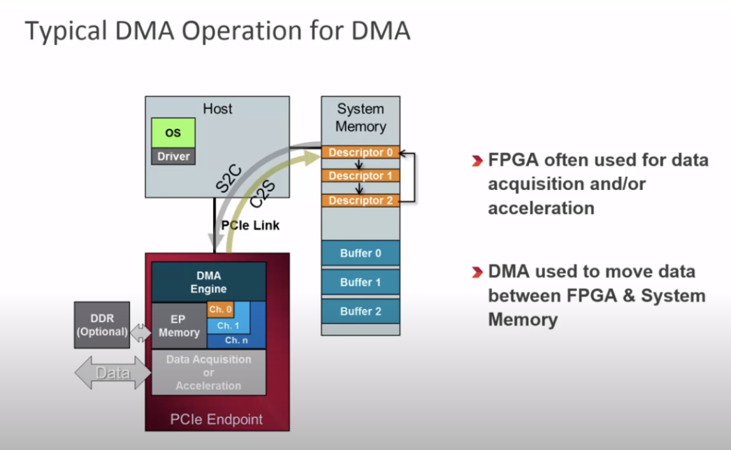
Figure 2: Typical DMA Operation Diagram
The XDMA Driver is what allows us to be able to read and write to these configuration registers, and Xilinx’s XDMA Driver Debugging guide is a great resource to understand exactly how it works. In brief, here is a short summary from the DMA PCIe User Guide that explains how the driver works to create a H2C transaction:
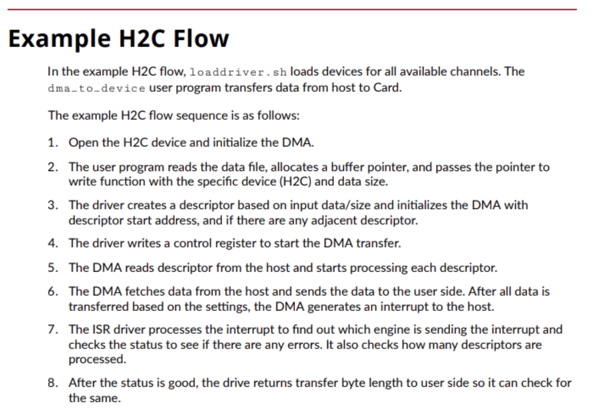
Figure 3: H2C Transaction
The process for a C2H Transfer is very similar to these steps, except that the data is being transferred from the user side to the host machine. These steps can be seen below:
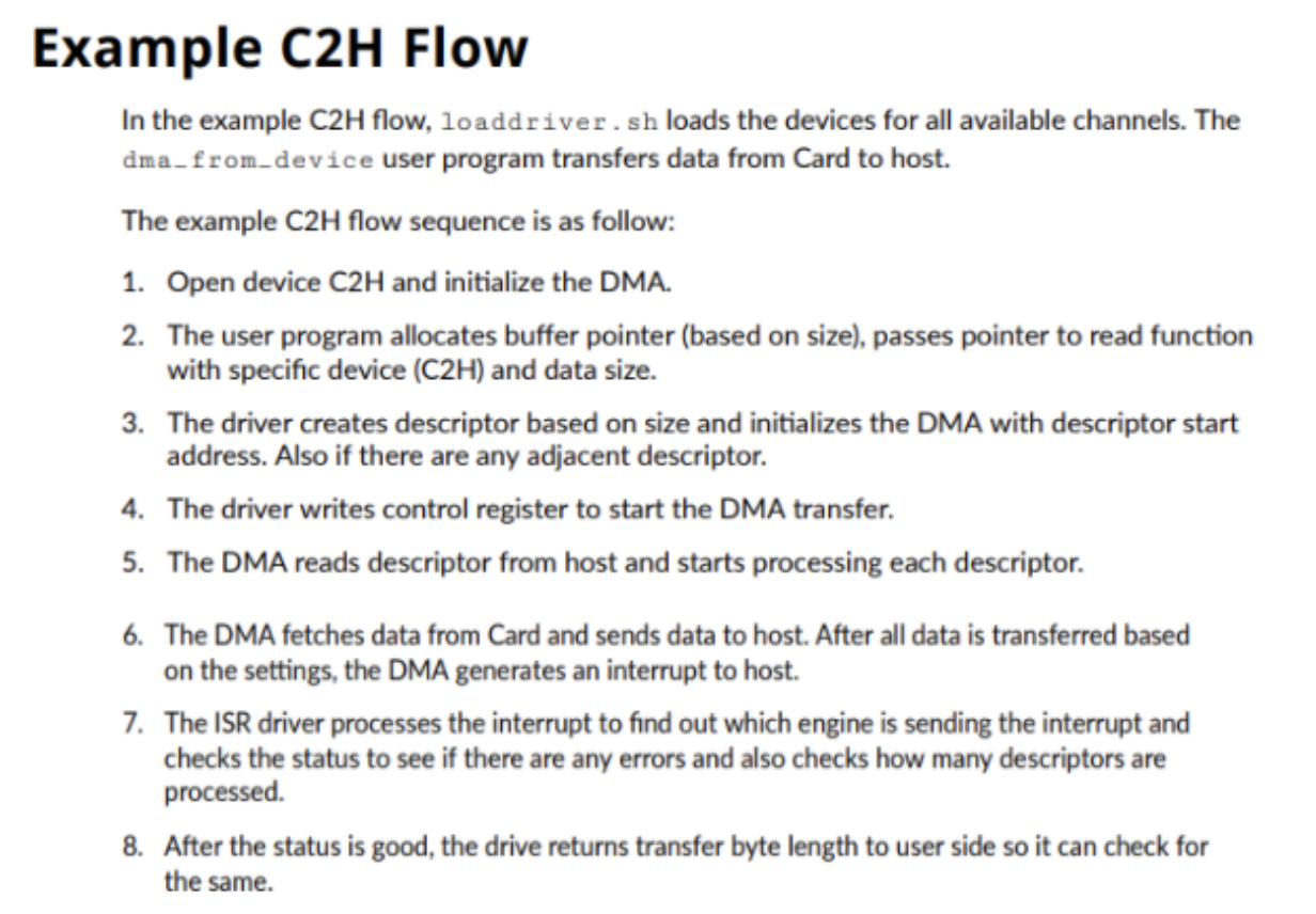
Figure 4: C2H Transaction
3.3. Configuring the DMA IP
The user configuration of the DMA/Bridge Subsystem for PCI Express IP is very similar to the AXI Memory Mapped to PCI Express IP. It can be customized by either selecting the IP in the IP Integrator tool or by inserting it into a block diagram. Here are some of the new customization options presented with this IP:
Basic tab:
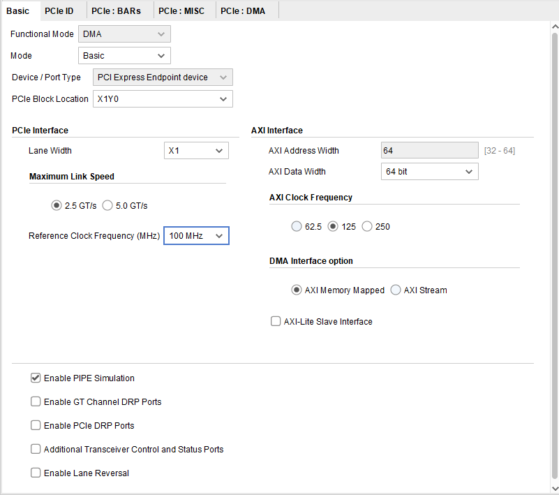
Figure 5: IP Configuration - “Basic” Tab
You can select whether you would like to use AXI Memory Mapped or AXI Stream for the DMA interface.
Just like the AXI Memory Mapped PCIe IP, you can also specify the lane width, link speed, AXI data width, AXI clock frequency, reference clock frequency, and external PIPE interface for faster simulations.
BARs tab:
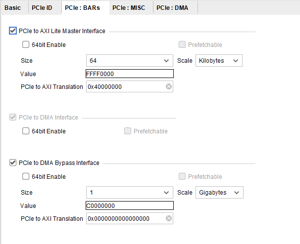
Figure 6: IP Configuration - “BARs” Tab
Here, you can choose to enable or disable the AXILite and AXI Bypass Base Address Registers (BARs), as well as specify the desired offset address and size.
Note
Based on your selections in this window, the BARs will be created according to this table from the Xilinx IP User Guide:
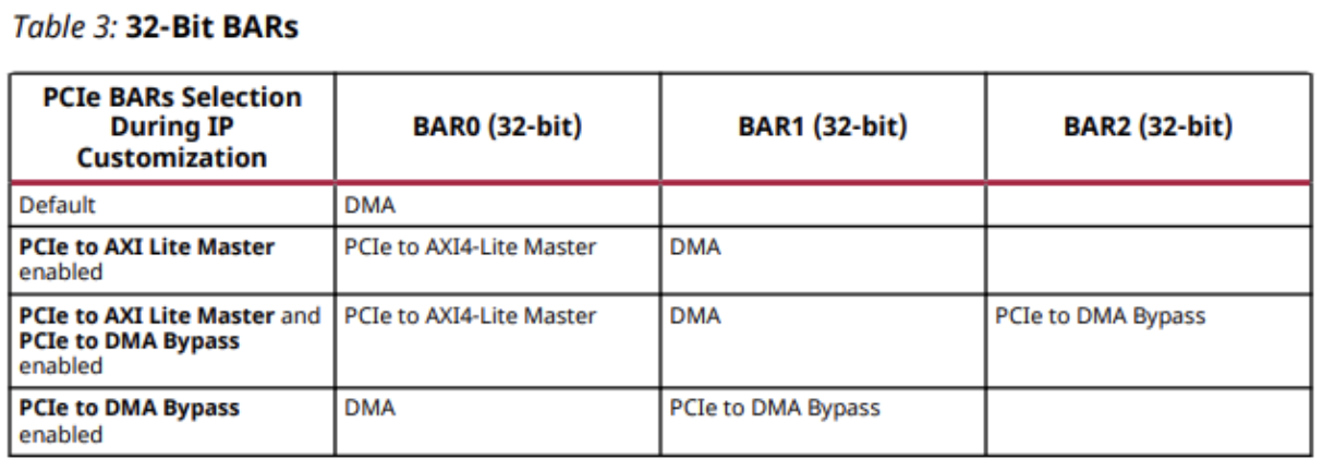
Figure 7: BAR Configurations
DMA tab:
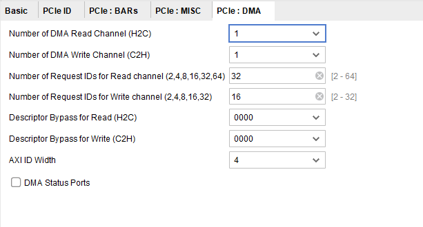
Figure 8: IP Configuration - “DMA” Tab
Here, you can select the number of DMA read and write channels, as well as specify other parameters related to DMA operation.
Seen below is an example configuration of this IP in a typical block diagram. This particular design was generated by the Xilinx “Run Block Automation” tool, and can be easily recreated by following these steps:
Open up a new block diagram and place the DMA /Bridge Subsystem for PCI Express IP into the page.
Click on the green banner at the top of the screen that says “Run Block Automation”, and then change the “Automation Level” to “Subsystem Level”.
Optionally, replace the AXI Interconnect with an AXI Smartconnect for more up-to-date designs.
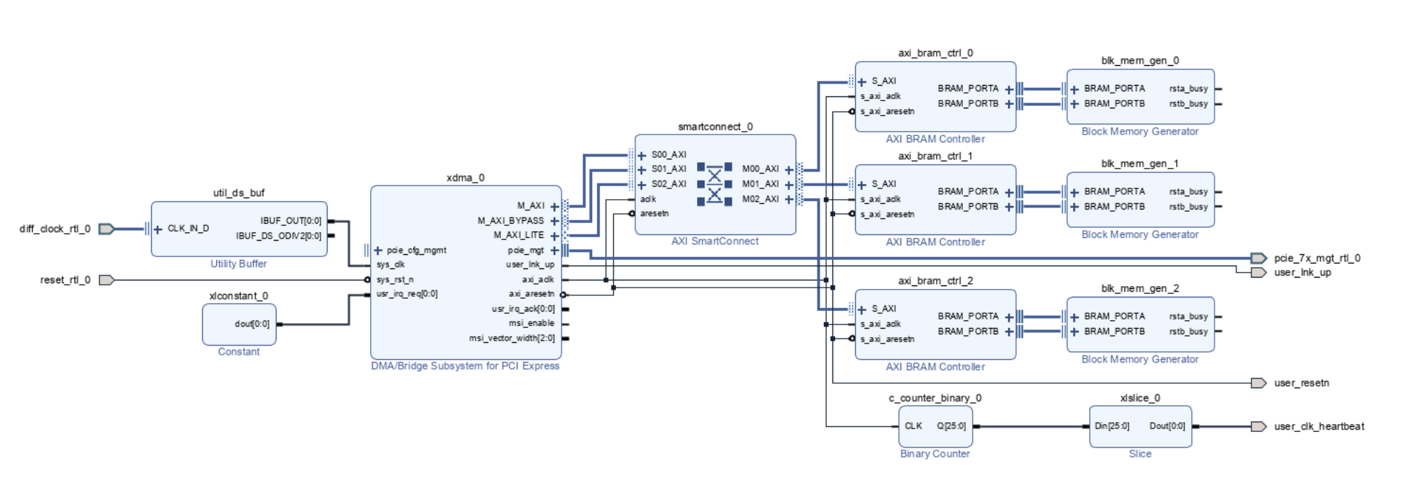
Figure 9: Example Block Diagram
As we can see from this design, our 100MHz differential reference clock needs to be connected through a IBUFDSGTE utility buffer before it can be connected to the sys_clk input of the IP. This was also the case for the AXI Memory Mapped to PCI Express IP. We also inserted a constant value of 0 to the usr_irq_req port in order to ensure that we are not accidentally sending any unwanted interrupts.
Unlike the AXI Memory Mapped to PCI Express IP, the sys_rst_n pin can be directly connected to the PERST (PCIe Reset) pin for an Active Low reset. Then, the axi_aresetn output should be used to reset all other components driven by the DMA PCIe IP (Smartconnects, BRAM, etc.).
The axi_aclk output port contains a 125MHz clock, which is the operating frequency of the DMA PCIe core. The external pins coming from the pcie_mgt output are what physically connect to the PCIe header to allow for the communication of Transaction Layer Packets (TLPs) from the host machine to the PCIe endpoint (FPGA). The user_link_up output port is a status port that goes high once a connection has been made between the host machine and the PCIe endpoint.
Lastly, the M_AXI port is what connects to the device(s) that you would like to interface using the DMA protocol, the M_AXI_BYPASS port is what connects to the device(s) that you would like to interface using standard AXI-full PIO protocol, and the M_AXI_LITE port is what connects to the device(s) that you would like to interface using AXILITE PIO protocol. In this specific case, we have an AXI BRAM controller connected to each of the three interfaces, and these are mapped into the AXI space as seen in the Address Editor image below:
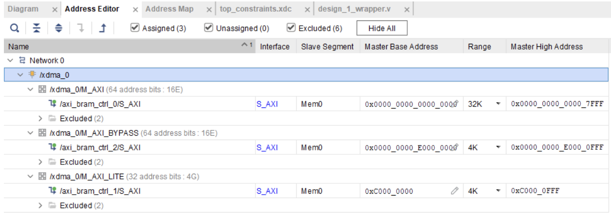
Figure 9: Example Block Diagram (Address Editor)