1. Building a Basic Simulation Environment (VC707)
1.1. Generating PCIe and MIG Example Designs
Now that we have experience generating and manipulating the PCIe and MIG example designs, we can start putting the pieces together - that is, building the basic infrastructure behind our FPGA emulation environment. The infrastructure will begin modifying Xilinx’s PCIe example design, as this will allow us to perform reads and writes to both DDR memory and a replaceable Device Under Test (DUT), as well as other on-board peripherals. This can be accomplished through the use of an AXI SmartConnect, or what is known as a a “NoC” in industry. You can read more about the SmartConnect IP and the AXI protocol here. We will give the DDR memory and the Device Under Test different offset addresses in the AXI memory space, and then we can decide which device the PCIe will read or write to by specifying the address of the transaction.
Note
For a refresher on generating the MIG example design or targeting the VC707 board, please see this MIG overview.
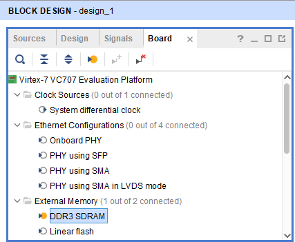
First, we will want to create a new Vivado project and select your preferred FPGA or board. For this article, we will be using the Xilinx VC707 board as our target. Then, open up a new block diagram. Under the Board tab, select the DDR3 SDRAM option.
This will insert a MIG into the block diagram, which we can edit by double clicking on the IP. If you are not using a board, generate a MIG 7 Series or equivalent IP using Xilinx’s IP integrator. For the MIG 7 Series, modify the following fields:
Important
Unless mentioned otherwise, leave all values default.
Desired Clock Period → 2500ps (400MHz)
Data Width → 64 bit (default)
AXI Data Width → 64 bit
Input Clock Period → 5000ps (200MHz)
Deselect any Additional Clocks
Addressing → Bank/Row/Column
System Clock → Differential
Reference Clock → Use System Clock
Reset → ACTIVE LOW
Uncheck the Box for DCI Cascade
Select Fixed Pinout, then select Validate for the given pinout
In the System Signals section:
Leave
sys_clk_pandsys_clk_nto their default pinsAssign
sys_rstto AR40 (push button)Assign
init_calib_completeto AM39 (LED)
Of course, the pinout will differ depending on the board or FPGA chosen. For more infomation on the VC707 board pinout, see this documentation from Xilinx here: UG885.
Once these modifications have been made, the MIG IP will regenerate. Then, generate the IP example design by right-clicking on the IP block and selecting Generate IP Example Design. As before, this will open up a project in Vivado with the MIG IP example design, which we can set aside for the moment.
Now, we will also need to generate the IP example design for the AXI Memory Mapped to PCI Express core.
Note
For a refresher on generating the AXI Memory Mapped to PCI Express example design, please see this PCIe overview.
Click on the + icon to add IP to the block design, then select AXI Memory Mapped to PCI Express. Make the following changes to the core:
Important
Unless specified, please leave everything as default.
Reference Clock Frequency → 100MHz
Check the box to enable External PIPE Interface (this helps to speed up the simulation time)
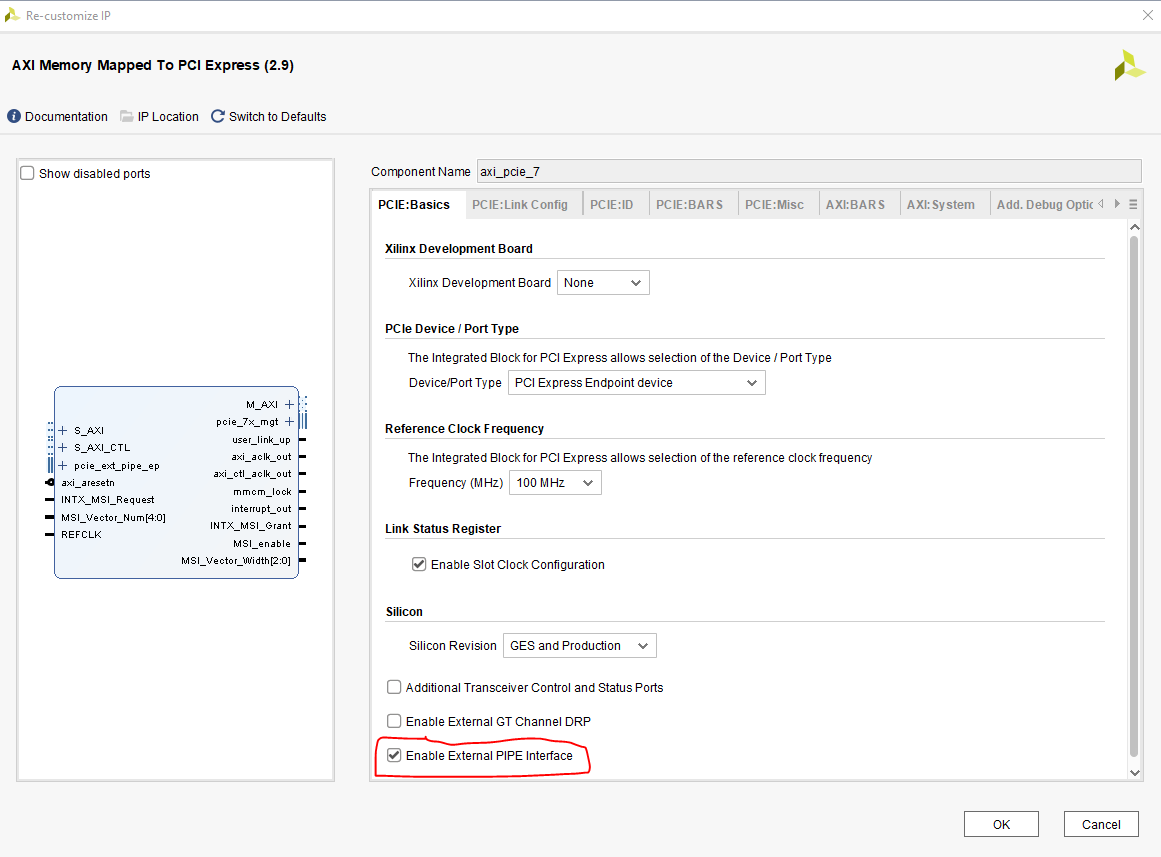
PCIE:Basics Customization
Lane Width → X8
Link Speed → 2.5GT/s
In the PCIE BARs section, ensure only 1 BAR is enabled and that it is 16KB in size with offset at address 0x00000000.
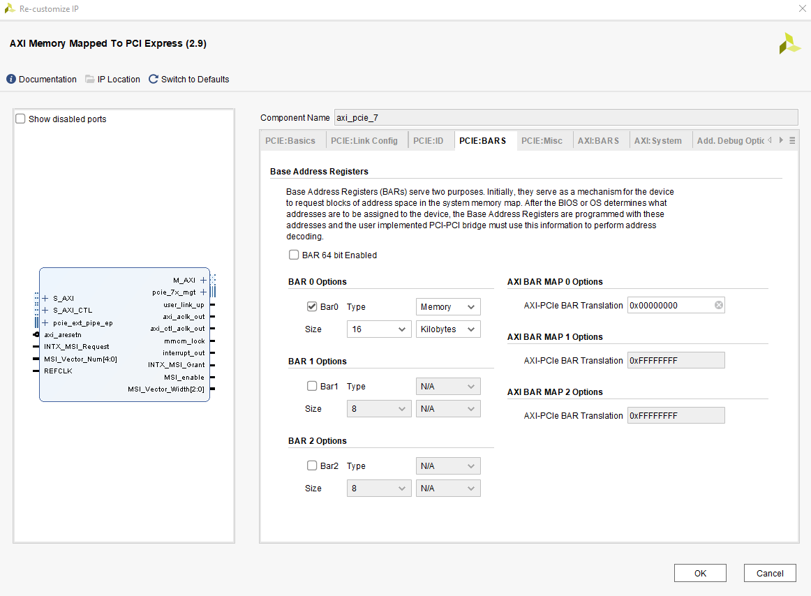
PCIE:BARS Customization
Once this core has been generated, generate an example design for this IP as well. Now that the example designs have been generated for both the MIG and the PCIE IPs, we are ready to move onto the next section.
1.2. Creating the Block Diagram
Like we did in the section 2.4 of the AXI MM to PCIe IP Overview,
the first step that we will do is comment out the BRAM instantiation from the top file of the PCIE example design
(xilinx_axi_pcie_ep.v). However, instead of inserting a MIG into its place, we are instead going to create
a new block diagram. In the end, this is what we want the block diagram to look like:
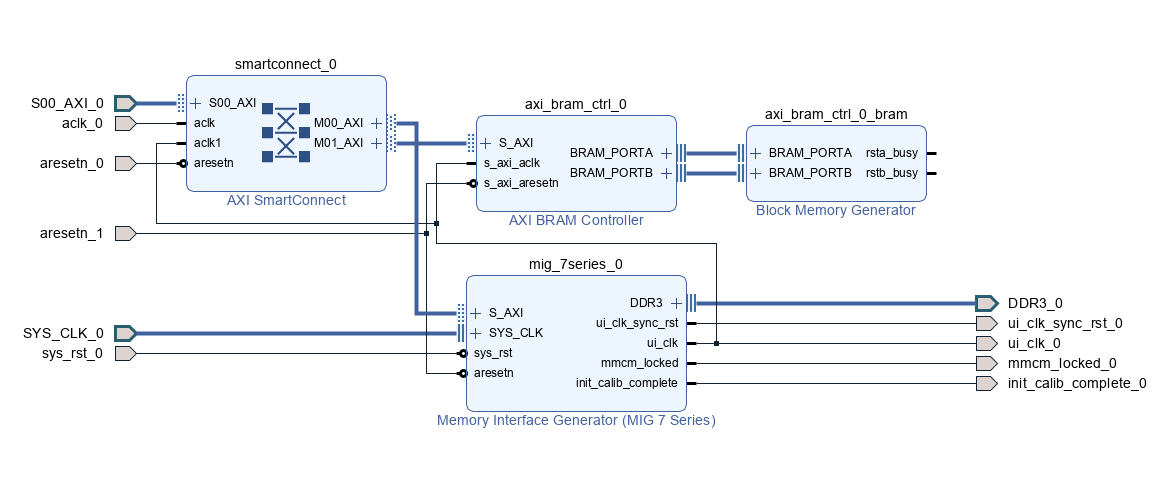
Combined block diagram
In order to create this block diagram, follow these instructions:
Add an AXI Smartconnect IP to the block design with two AXI Master outputs and one AXI Slave input. Make sure that the data width is set to at least 32 bits, and make sure that there are two clock inputs.
Make the S00_AXI, aclk, and aresetn ports external, as these will connect back into our PCIe core.
Add a MIG 7 Series IP to the block design from the Board tab, and make sure to customize it in the EXACT SAME way as the MIG you customized in the previous section. This will ensure that the example design we generated will have the correct parameters associated with it.
Make the
SYS_CLK,sys_rst,aresetn,DDR3,ui_clk_sync_rst,ui_clk_,mmcm_locked, andinit_calib_completepins external, as these will be handled by our MIG example design. TheSYS_CLKandDDR3pins should already be external, but to keep the same naming convention, delete the previous external connections, and then right-click to make them external again.Add an AXI BRAM controller IP to the block design, and make sure to set the interface type to AXILite and Data Width to 32 bits. This BRAM represents the replaceable DUT that we should be able to exchange with a custom design later.
Connect the
M00_AXIport from the Smartconnect to theS_AXIport on the MIG, and connect the M01_AXI port from the Smartconnect to the S_AXI port on the BRAM controller.Connect the
ui_clkfrom the MIG to theaclk1port on the Smartconnect and thes_axi_aclkport on the BRAM controller. This way, the example DUT will be in the same clock domain as the MIG.Connect the
s_axi_aresetnport on the BRAM controller to the external aresetn signal going into the MIG. This way, the example DUT reset will be synchronous with the MIG reset.Finally, there should be an option at the top of the screen to Run Connection Automation, and doing this should insert the Block Memory Generator, which will be attached to the BRAM controller.
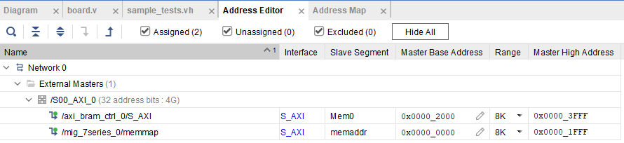
Now that the block diagram has been created, we will need to use the address editor to assign the MIG and BRAM locations in the AXI memory space. Click on the Address Editor tab, and edit the offset addresses as follows:
MIG: size 8KB, range: 0x0000_0000 to 0x0000_1FFF
BRAM: size 8KB, range: 0x2000_3FFF
Address Editor for MIG and BRAM
If we click on the Address Map tab, then we can even see a layout of the memory mapping:
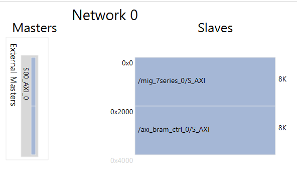
Address Map for MIG and BRAM
Since we configured the PCIe to have a 16KB BAR from address 0x0000_0000 to 0x0000_3FFF, we should now be able to access both of our AXI slaves from within the PCIE memory space.
Finally, we can go ahead and right-click on our block diagram and select validate design. There might be a warning that the resets are not synchronous - this is because we have not connected the PCIe IP to the design yet, so we can ignore this for now. Once Validation is successful, we will need to right-click on the block design under the Sources menu, and select Create HDL Wrapper. Just like before, this will generate an RTL wrapper file for this block diagram, which we can instantiate into our PCIe example design in the next section.
1.3. Connecting it All Together
Similar to section 2.4, we will now need to instantiate our block diagram into the PCIe example design. Since this process has several steps involved with it, we will include the design, constraints, and simulation top file here. This next section will be a brief overview of the steps needed to combine the PCIe example design, the MIG example design, and the block diagram. This has already been done for you in this case (just download the files), but it is highly recommended that you follow along and try to understand what modifications were made in each step.
Important
You can download our design top file here.
Important
You can download our constraints file here.
Important
You can download our simulation top file here.
First, we will need to correctly instantiate the block design wrapper file into the PCIe example top file. In order to do this, we can locate where we commented out the old BRAM instantiation, and instead instantiate the block design.
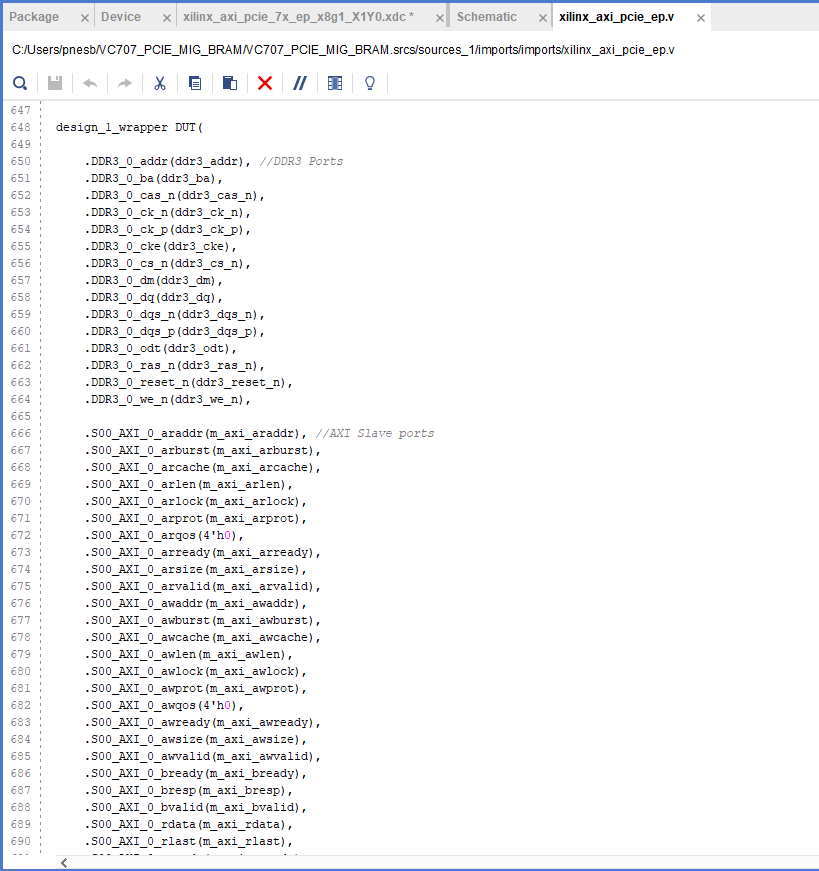
Instantiating the Block Diagram (1)
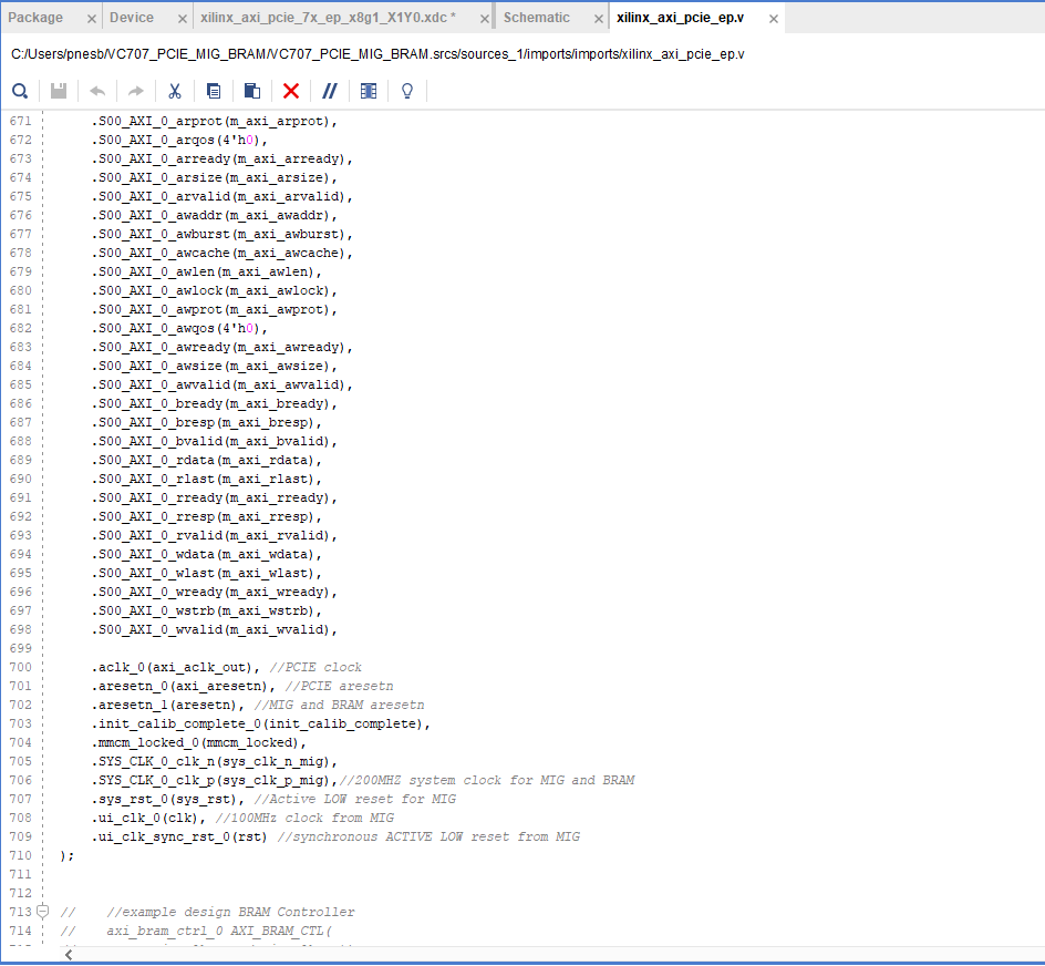
Instantiating the Block Diagram (2)
Then, we will need to copy all of the relevant parameters, wires, functions, inputs, and outputs from the MIG example design top file into the PCIe example design top file. For more a deeper explanation on this, see section 2.4 on the AXI MM to PCIe IP Overview tab.
Note
The following fields had to be changed because of already existing fields in the PCIe example design.
Parameters:
TCQ→TCQ_MIGInputs:
sys_clk_n→sys_clk_n_migOutputs:
sys_clk_p→sys_clk_p_mig
Make sure to copy over the statement that synchronizes the MIG reset:
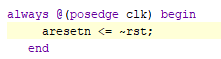
Copy over the MIG Reset Statement
Then, we will need to copy over the top-level constraints from the MIG example design and paste them into the top-level constraints file for the PCIe example design. The top level constraints for each project can be found under the Constraints tab in the Sources menu.
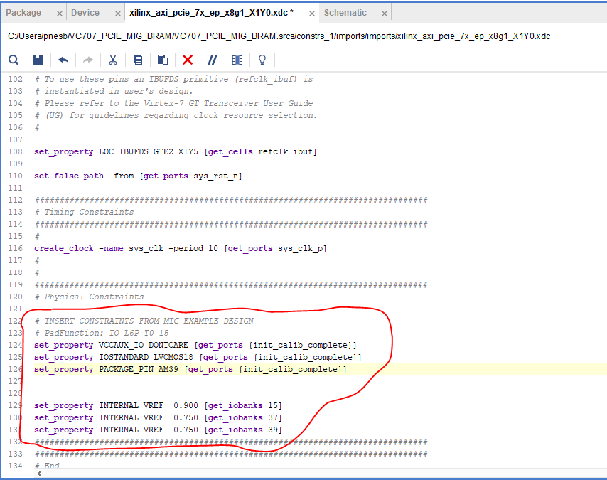
Copy over top-level constraints from MIG Example Design
Once the top file and the constraints file have been modified, then we can run synthesis and implementation to ensure that there are no errors in our design. Refer to the TCL console and the Xilinx forums for help with debugging, as every board/FPGA has different parameters, or cross reference your design and constraints top file with the provided example files above.
Once synthesis and implementation are complete, your schematic should look something like this. Once synthesis and implementation are complete, we can now move on to the next section.
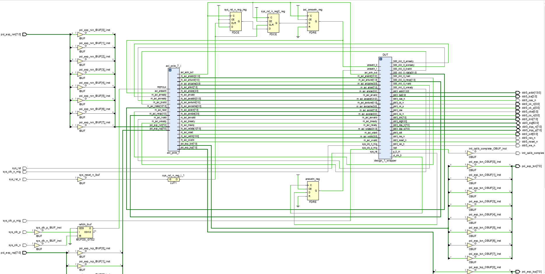
Example schematic of infrastructure Block Diagram (BD)
1.4. Modifying and Running the Simulation
Just like the example in section 2.5 of the AXI MM to PCIE IP Overview, the first step
to running our simulation is to import the correct simulation files from the MIG example project (ddr3_model.sv,
ddr3_model_parameters.vh, and wiredly.v). For more information on how to import these files, please reference that section.
As an additional reference, these files have also been attached below.
Important
ddr3_model.sv file available here.
Important
ddr3_model_parameters.vh file available here.
Important
wiredly.v file available here.
Now, we will need to edit our simulation top file to accommodate the MIG and DDR3 memory model, as well as include our block diagram from earlier. In this case, you can simply download the above files and import them into your design, but it is again recommended that you read through and try to understand the modifications made below.
Some notes about the modifications made to the PCIe example design top file:
Parameters changed:
TCQ→TCQ_MIG(duplicate name)ADDR_WIDTH→ADDR_WIDTH_MIG(duplicate name)RESET_PERIOD= 100 (convert to nanoseconds)
Wires/Regs changed:
sys_rst_n→sys_rst_n_mig(duplicate name)
Variables changed:
In the memory model instantiation, the variable i had to be changed to s due to a duplicate name
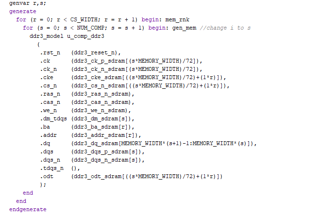
Changing variable ‘i’ to ‘s’ due to duplicate name
MIG input system and reference clocks: - Due to timescale issue (MIG simulation top file is in picoseconds, PCIe simulation top file is in nanoseconds),
We were forced to change the system and reference clocks to run at 250MHz instead of 200MHz (4ns period instead of 5ns period). This in turn causes the MIG ui_clk to run at 125MHz instead of 100MHz. However, everything in the simulation should still run fine.
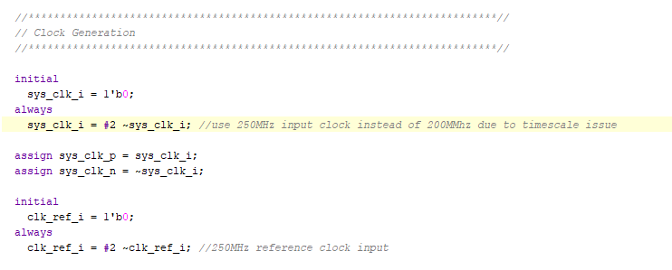
Change system and reference clock to 250MHz
Instantiations included:
Top file from design sources
DDR3 memory model
Wire delay modules
In order to determine when init_calib_complete goes HIGH for the MIG, a simple check that displays “MIG Calibration Done” when this event occurs was added.
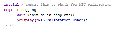
Finished MIG calibration
Now, if we were to click Run Behavioral Simulation, the standard PCIe example simulation would run, which would simply
perform a read and a write to address 0x0000_0010. For debugging purposes, it may be smart to try and run this simulation to make
sure that everything is set up properly. However, we want to be able to read and write our own data to our own specific addresses.
In order to do this, we will need to edit the simulation header file called sample_tests1.vh. This file can be located in the
Verilog Header folder within Simulation Sources. As a reference, we have also attached our own sample_tests1.vh
file below for you to download.
Important
You can download our custom simulation header file here.
Under the comment that says “MEM 32 SPACE” in the BAR Testing section, a 60us delay is included to allow for the MIG to
finish calibrating before attempting to read and write from it. The predefined tasks TSK_TX_BAR_WRITE and TSK_TX_BAR_READ
perform the custom reads and writes. The definitions of these tasks can be found in the pci_exp_usrapp_tx.v file contained within
the Root Port simulation model.
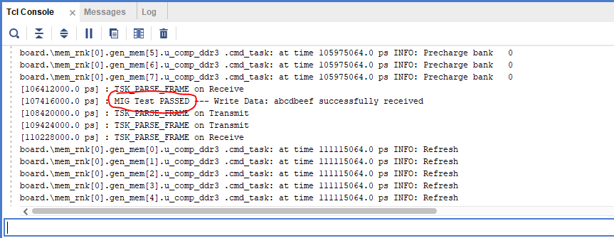
To test the MIG, the sample data 0xABCD_BEEF was written to address 0x0000_0010, which corresponds to address 0x0000_00010
on the MIG. If the read data equals the written data, then the message MIG Test Passed will appear in the TCL console.
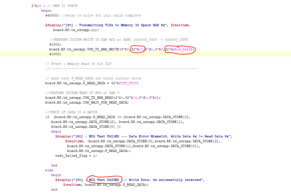
MIG Test Passed
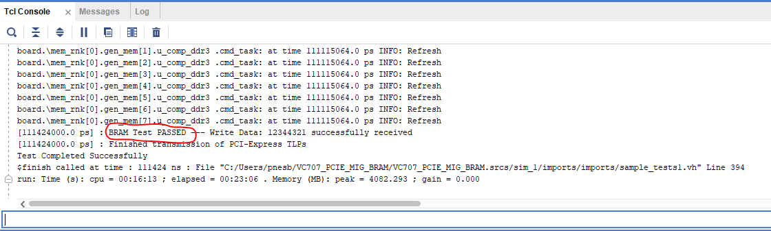
In order to test the BRAM controller (aka the DUT), I sent the data 0x1234_4321 to address 0x0000_2000, which should correspond
to address 0x0000_0000 on the BRAM controller. If the read data equals the written data, then the message “BRAM Test Passed” will
appear in the TCL Console.
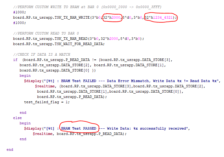
BRAM Custom Test
Now that we have built our simulation environment, we can go ahead and Run Behavioral Simulation.
Note
If the simulation fails to launch, the TCL console will direct you to the location of a log file that will provide more specific error-related information for debugging.
The simulation should automatically pause itself after 1 nanosecond, and this is a good time to add the desired waveform signals into the simulation window. This can be done by navigating to the Scope window, right clicking on the signals you would like to see, and then clicking Add to Wave Window. I would personally recommend adding the signals from the XILINX_AXIPCIE_EP file, the axi_bram_ctrl_0 file, and the mig_7series_0 file as shown in the image below.
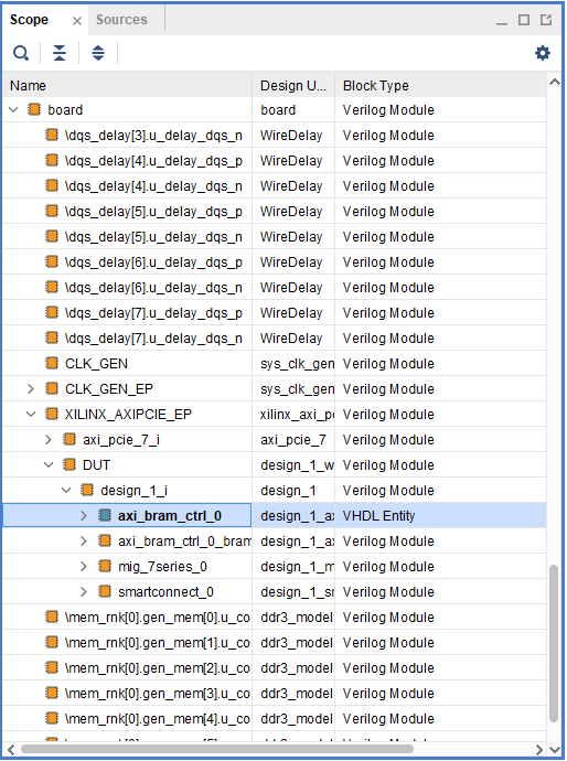
BRAM Scope
Once we’ve added the correct signals, we can click on the green play button at the top left corner of the screen to resume the simulation.
Note
If the simulation stops early (before 100us) due to a timeout error from one of the PCIE root port files, we can go ahead and just click the green play button to force the simulation to resume anyways. If this becomes bothersome, we can comment out the timeout error from occurring like this:
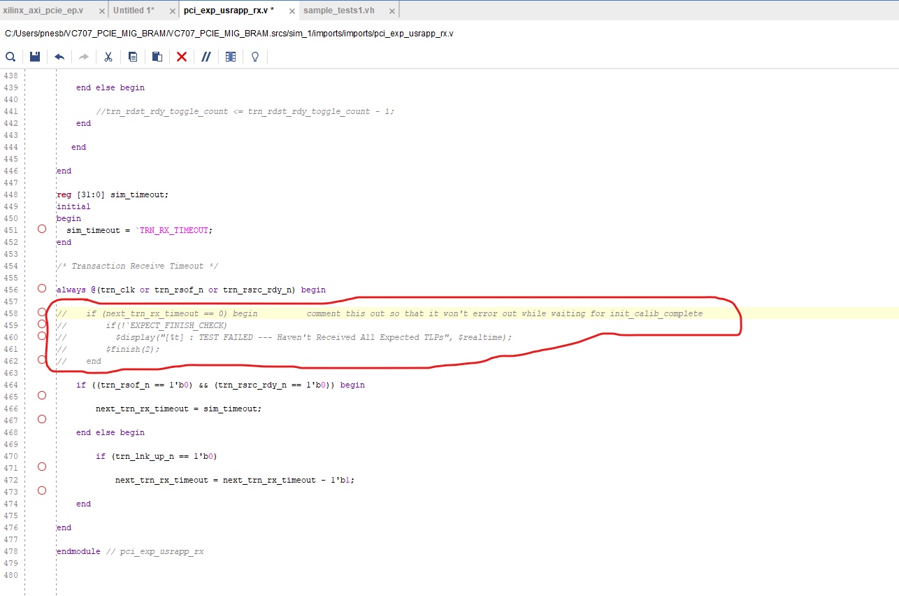
Comment out timeout error
Finally, the simulation should conclude around 110 us, and if you see the following messages in the TCL console, then the simulation was a success!
MIG Test Passed
BRAM Test Passed
Additionally, we can view the AXI transactions in the simulation window. One important thing to notice is that the PCIE sent a write transaction
to address 0x0000_2000 for the BRAM test, but because of the address offset that we specified for the BRAM controller back in the block diagram
stage, the BRAM received this write request at address 0x0000_0000. This is how we will be able to use the PCIE to read and write to multiple
slave devices simultaneously.
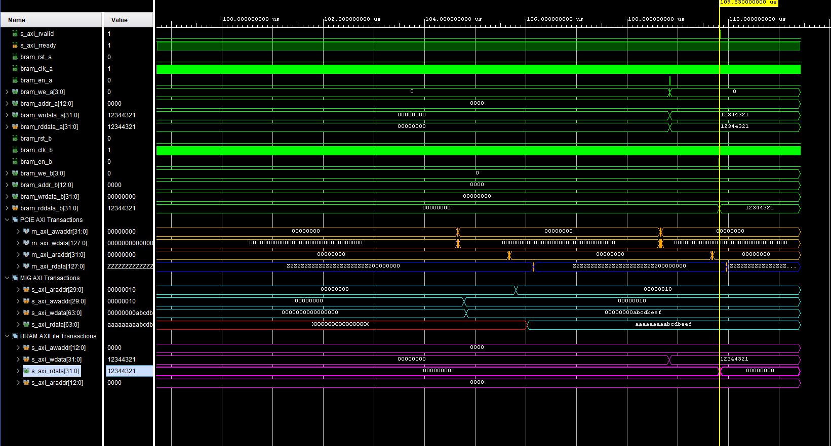
BRAM MIG Waveform
1.5. Checking Timing, Viewing Power Reports, Monitoring I/O Placement:
After running through synthesis and implementation, Vivado provides us with several tools that we can use to monitor important factors of our design such as timing, power, and I/O placement.
The first category that we can take a look at is the Timing section. In this Design Timing Summary, we can see several aspects of our timing report, such as the total number of endpoints, worst negative slack, and most importantly, whether our device meets timing or not. In this example, we can see that our device successfully meets all of the timing requirements as shown in the figure below.
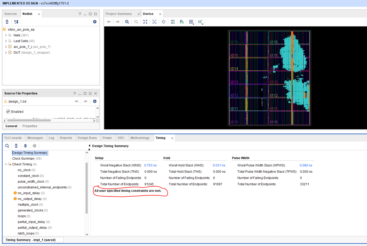
Timing Summary Met
If we click on the Check Timing tab on the left side of the screen, it will show us a more detailed layout of the timing summary
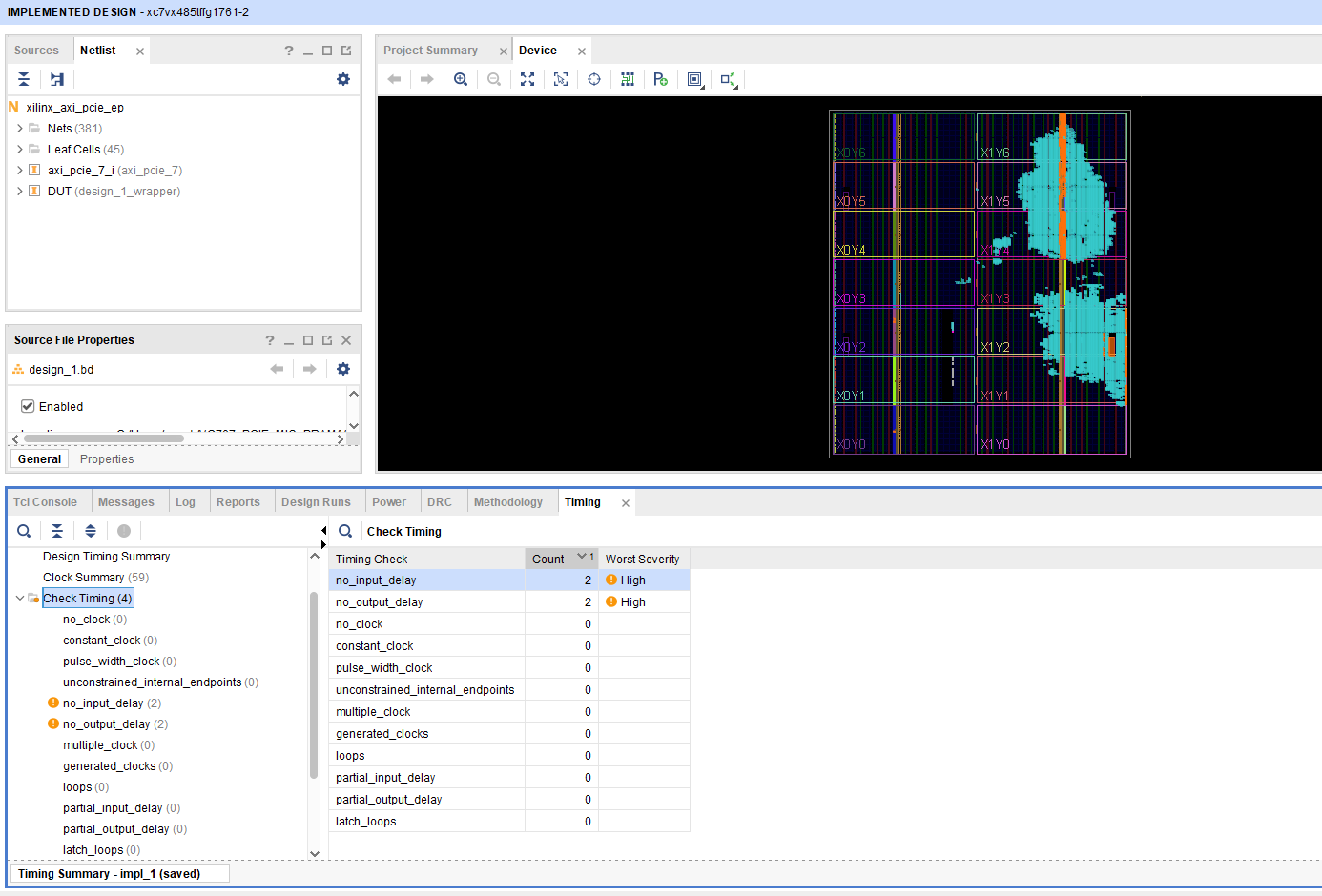
Check Timing Summary
In this case, we can see that there are 4 total errors with our timing: 2 no_input_delays and 2 no_output_delays. If we click on
those respective sections on the left side of the screen, we can see which exact ports are afflicted by these errors. However, since all
of the timing constraints are still met within the design, it is alright to ignore these errors.
This is also the place where we would see if any clocks were not properly constrained. If this were the case, we would usually see a large amount of errors under the no_clock category.
If any of these errors were preventing our design from meeting timing, we can use the Vivado Timing Constraints Wizard to help us
write clock constraints to fix these errors. In order to access the wizard, open up the implemented design, click on the Tools menu
at the very top of the screen, and then click on Timing → Constraints Wizard.
Note
If you do decide to use the timing constraints wizard, it will automatically write the constraints for you based on the clocks you need to define, and it will OVERWRITE any constraints that you already have in your target constraints file. Personally, I would recommend copying and pasting the text from your target constraints file somewhere safe before running the wizard.
To check the Vivado Power Report for our design, click on the Power tab within the implemented design.
From here, we can see additional information relevant to the on-chip power required for implementation, as well as the power distribution for each FPGA primitive used in order to build the design (clocks, PLLs, I/O, BRAM, etc.)
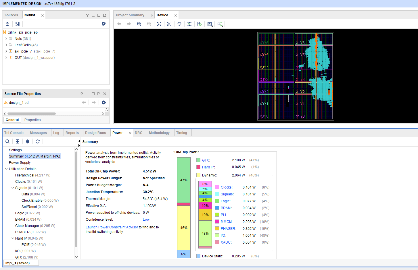
Check Power Summary
In this case, we can see that the total on-chip power required is 4.512 Watts, which is broken down into the individual FPGA components in the diagram to the right.
One other very handy tool that Vivado provides for us is the ability to view and modify the I/O planning of the design. In order to access the I/O planning page, open up the implemented design, select the Layout menu at the very top of the screen, and then select I/O Planning.
This should open up a new tab on the Implemented design called I/O Ports, and navigating through this tab allows you to view all of the pin
locations defined within your constraints, as well as their respective location within the FPGA
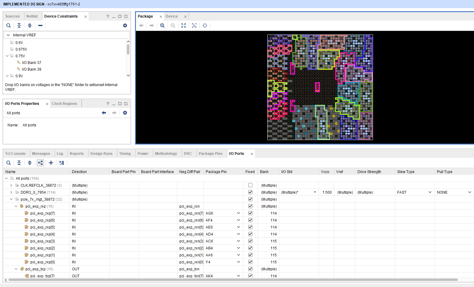
IO Pin Planning
Similar to the Timing Constraints Wizard, we can manually assign the input/output ports of our designs to any respective package pin port, and the Vivado tool will write the constraints for us. However, it will also overwrite any previously written constraints, so always make sure to copy and paste your top level constraints somewhere safe before saving any edits.
Other things that we can do within this window include setting the I/O Std type and enabling/disabling pullup resistors.