2. Creating an Advanced Custom AXI Descriptor IP
This documentation is a continuation of Creating a Custom AXI IP Core. The purpose of this documentation is to take the counter previously created and make it more advanced by allowing it to communicate with memory. In this documentation the DUT will utilize BRAM through the standard IP catalog provided through Xilinx.
2.1. Features of Advanced DUT
- Features of the Descriptor DUT:
Write the current count value to memory (BRAM addr: 200)
Read in an initial count value from memory (BRAM addr: 204 [7:0])
Read in increment or decrement mode from memory (BRAM addr: 204 [8])
Prompt the DUT to initiate a write or read transaction to memory
External
count_outbus port
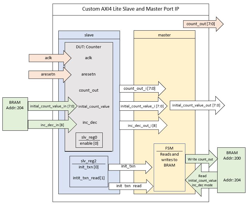
Block Diagram of the Descriptor Counter
Here is a brief description of the counter’s operation:
The initial counter we previously made takes in a clock and reset signal. When the counter is enabled,
it will increment the 8-bit count value on every clock cycle. When reset is activated, the
counter value will reset to the initial count value.
This more advanced counter will have both a AXI master and a AXI slave when packaged. The slave will take in values/commands and pass them to the master. The master will then take these commands and instantiate them into memory.
In order for the DUT to obtain and send values to/from memory, it is necessary to create some
intermediate variables. For example, when the initial count value is read in from memory, we will refer
to this as initial_count_value_i in the top file, initial_count_value_in in the slave file,
and initial_count_value_out in the master file.
When reading in a value from memory, it obtains data from the rdata bus. This means that the data
must already be on the rdata bus for it to be implemented. For example, when you first want to use
the counter, you need to send a 9-bit value directly to BRAM address 204. You would then write to
initiate the DUT to perform a read transaction so it will read from BRAM and the data will be
loaded onto rdata, then you can enable the counter.
The value that is read will be 32 bits in this example. However the only bits that are important to this counter are the lower 9 bits ([8:0]). The last 8 bits ([7:0]) are the initial count value and the 9th bit ([8]) is the increment or decrement mode. Increment is low active.
In this specific example, I made the address editor BRAM set to addr 0 and the DUT to addr 4000_0000. In addition when I edited the custom IP, I set a slave address offset to address 200. This means that when I initiate the counter to write to BRAM, even though the BRAM is at 0000_0000, the value will be written to addr 200 because of this offset.
2.2. Editing the Descriptor Counter IP
To edit the counter IP, we will directly edit the top file.
Important
If you wish to download the top file directly, go here.
Add port
output port [7:0] count_out.
2. Comment out line port for master input wire m00_axi_init_axi_txn because we want this to
be controlled manually from an external port by user.
3. Before the slave instantiation, add the following wires. These are necessary because they are used in the instantiation below so we need to create them before using them.
//create wires for instantiation below
wire m00_axi_init_axi_txn;
wire [7:0] count_out_i;
wire [7:0] initial_count_value_i;
wire m00_axi_init_read_txn;
In the slave instantiation insert the following:
.init_txn_read(m00_axi_init_read_txn),
.init_txn(m00_axi_init_axi_txn),
.count_out_i(count_out_i),
.initial_count_value_in(initial_count_value_i) //connect initial_count_value from Master output to Slave input
In the master instantiation, add the following lines:
.init_axi_txn_read(m00_axi_init_read_txn),
.count_out_i(count_out_i),
.count_out(count_out),
.initial_count_value_out(initial_count_value_i) //connect initial_count_value from Master output to Slave input
Slave File:
Important
If you wish to download the top file directly, go here.
Add the following user ports:
output wire[7:0] count_out_i,
output wire init_txn,
output wire init_txn_read, //make it an external port
input wire[7:0] initial_count_value_in, //initial count value sent from rdata
Add the user logic at the bottom of this file. In this example we are instantiating a counter as follows:
counter DUT(
        .aclk (S_AXI_ACLK),
        .enable (slv_reg0[0]), //set bit 0 of slv_reg0 to enable
        .aresetn (S_AXI_ARESETN), //reset as axi slave reset
        .inc_dec (slv_reg0[1]), //set bit 1 of slv reg0 as inc/dec setting
        .start_value (initial_count_value_in), //slv_reg1 bits 7-0 to store start value
        .count_out (count_out_i) //count value
        );
assign init_txn = slv_reg2[0];
assign init_txn_read =slv_reg2[1];
Master File:
Important
If you wish to download the top file directly, go here.
Insert the following ports:
input wire [7:0] count_out_i,//intermediate count value
output wire [7:0] count_out,
input wire init_axi_txn_read, //signal to initiate a read
output wire[7:0] initial_count_value_out, // output signal for initial counter value
2. Customize the master file to work as desired. In this case we changed the finite state machine and created an initiate read txn that will operate separate from initiating a write txn. The code is below and the changes made are highlighted:
`timescale 1 ns / 1 ps
module myip_counter_master_read_v1_0_M00_AXI #
(
// Users to add parameters here
// User parameters ends
// Do not modify the parameters beyond this line
// The master will start generating data from the C_M_START_DATA_VALUE value
parameter C_M_START_DATA_VALUE = 32'h00000000,
// The master requires a target slave base address.
// The master will initiate read and write transactions on the slave with base address specified here as a parameter.
parameter C_M_TARGET_SLAVE_BASE_ADDR = :guilabel:`32'h00000200`,
// Width of M_AXI address bus.
// The master generates the read and write addresses of width specified as C_M_AXI_ADDR_WIDTH.
parameter integer C_M_AXI_ADDR_WIDTH = 32,
// Width of M_AXI data bus.
// The master issues write data and accept read data where the width of the data bus is C_M_AXI_DATA_WIDTH
parameter integer C_M_AXI_DATA_WIDTH = 32,
// Transaction number is the number of write
// and read transactions the master will perform as a part of this example memory test.
parameter integer C_M_TRANSACTIONS_NUM = 4
)
(
// Users to add ports here
:guilabel:`input wire [7:0] count_out_i,//intermediate count value
output wire [7:0] count_out,
input wire init_axi_txn_read, //signal to initiate a read
output wire[7:0] initial_count_value_out, // output signal for initial counter value`
// User ports ends
// Do not modify the ports beyond this line
// Initiate AXI transactions
:guilabel:`input wire INIT_AXI_TXN,`
// Asserts when ERROR is detected
output reg ERROR,
// Asserts when AXI transactions is complete
output wire TXN_DONE,
// AXI clock signal
input wire M_AXI_ACLK,
// AXI active low reset signal
input wire M_AXI_ARESETN,
// Master Interface Write Address Channel ports. Write address (issued by master)
output wire [C_M_AXI_ADDR_WIDTH-1 : 0] M_AXI_AWADDR,
// Write channel Protection type.
// This signal indicates the privilege and security level of the transaction,
// and whether the transaction is a data access or an instruction access.
output wire [2 : 0] M_AXI_AWPROT,
// Write address valid.
// This signal indicates that the master signaling valid write address and control information.
output wire M_AXI_AWVALID,
// Write address ready.
// This signal indicates that the slave is ready to accept an address and associated control signals.
input wire M_AXI_AWREADY,
// Master Interface Write Data Channel ports. Write data (issued by master)
output wire [C_M_AXI_DATA_WIDTH-1 : 0] M_AXI_WDATA,
// Write strobes.
// This signal indicates which byte lanes hold valid data.
// There is one write strobe bit for each eight bits of the write data bus.
output wire [C_M_AXI_DATA_WIDTH/8-1 : 0] M_AXI_WSTRB,
// Write valid. This signal indicates that valid write data and strobes are available.
output wire M_AXI_WVALID,
// Write ready. This signal indicates that the slave can accept the write data.
input wire M_AXI_WREADY,
// Master Interface Write Response Channel ports.
// This signal indicates the status of the write transaction.
input wire [1 : 0] M_AXI_BRESP,
// Write response valid.
// This signal indicates that the channel is signaling a valid write response
input wire M_AXI_BVALID,
// Response ready. This signal indicates that the master can accept a write response.
output wire M_AXI_BREADY,
// Master Interface Read Address Channel ports. Read address (issued by master)
output wire [C_M_AXI_ADDR_WIDTH-1 : 0] M_AXI_ARADDR,
// Protection type.
// This signal indicates the privilege and security level of the transaction,
// and whether the transaction is a data access or an instruction access.
output wire [2 : 0] M_AXI_ARPROT,
// Read address valid.
// This signal indicates that the channel is signaling valid read address and control information.
output wire M_AXI_ARVALID,
// Read address ready.
// This signal indicates that the slave is ready to accept an address and associated control signals.
input wire M_AXI_ARREADY,
// Master Interface Read Data Channel ports. Read data (issued by slave)
input wire [C_M_AXI_DATA_WIDTH-1 : 0] M_AXI_RDATA,
// Read response. This signal indicates the status of the read transfer.
input wire [1 : 0] M_AXI_RRESP,
// Read valid. This signal indicates that the channel is signaling the required read data.
input wire M_AXI_RVALID,
// Read ready. This signal indicates that the master can accept the read data and response information.
output wire M_AXI_RREADY
);
:guilabel:`assign initial_count_value_out = M_AXI_RDATA[7:0];`
// function called clogb2 that returns an integer which has the
// value of the ceiling of the log base 2
// function called clogb2 that returns an integer which has the
// value of the ceiling of the log base 2
function integer clogb2 (input integer bit_depth);
begin
for(clogb2=0; bit_depth>0; clogb2=clogb2+1)
bit_depth = bit_depth >> 1;
end
endfunction
// TRANS_NUM_BITS is the width of the index counter for
// number of write or read transaction.
localparam integer TRANS_NUM_BITS = clogb2(C_M_TRANSACTIONS_NUM-1);
// Example State machine to initialize counter, initialize write transactions,
// initialize read transactions and comparison of read data with the
// written data words.
parameter [1:0] IDLE = 2'b00, // This state initiates AXI4Lite transaction
// after the state machine changes state to INIT_WRITE
// when there is 0 to 1 transition on INIT_AXI_TXN
INIT_WRITE = 2'b01, // This state initializes write transaction,
// once writes are done, the state machine
// changes state to INIT_READ
INIT_READ = 2'b10, // This state initializes read transaction
// once reads are done, the state machine
// changes state to INIT_COMPARE
INIT_COMPARE = 2'b11; // This state issues the status of comparison
// of the written data with the read data
reg [1:0] mst_exec_state;
// AXI4LITE signals
//write address valid
reg axi_awvalid;
//write data valid
reg axi_wvalid;
//read address valid
reg axi_arvalid;
//read data acceptance
reg axi_rready;
//write response acceptance
reg axi_bready;
//write address
reg [C_M_AXI_ADDR_WIDTH-1 : 0] axi_awaddr;
//write data
reg [C_M_AXI_DATA_WIDTH-1 : 0] axi_wdata;
//read addresss
reg [C_M_AXI_ADDR_WIDTH-1 : 0] axi_araddr;
//Asserts when there is a write response error
wire write_resp_error;
//Asserts when there is a read response error
wire read_resp_error;
//A pulse to initiate a write transaction
reg start_single_write;
//A pulse to initiate a read transaction
reg start_single_read;
//Asserts when a single beat write transaction is issued and remains asserted till the completion of write trasaction.
reg write_issued;
//Asserts when a single beat read transaction is issued and remains asserted till the completion of read trasaction.
reg read_issued;
//flag that marks the completion of write trasactions. The number of write transaction is user selected by the parameter C_M_TRANSACTIONS_NUM.
reg writes_done;
//flag that marks the completion of read trasactions. The number of read transaction is user selected by the parameter C_M_TRANSACTIONS_NUM
reg reads_done;
//The error register is asserted when any of the write response error, read response error or the data mismatch flags are asserted.
reg error_reg;
//index counter to track the number of write transaction issued
reg [TRANS_NUM_BITS : 0] write_index;
//index counter to track the number of read transaction issued
reg [TRANS_NUM_BITS : 0] read_index;
//Expected read data used to compare with the read data.
reg [C_M_AXI_DATA_WIDTH-1 : 0] expected_rdata;
//Flag marks the completion of comparison of the read data with the expected read data
reg compare_done;
//This flag is asserted when there is a mismatch of the read data with the expected read data.
reg read_mismatch;
//Flag is asserted when the write index reaches the last write transction number
reg last_write;
//Flag is asserted when the read index reaches the last read transction number
reg last_read;
reg init_txn_ff;
reg init_txn_ff2;
reg init_txn_edge;
wire init_txn_pulse;
//added registers for init_txn_read
:guilabel:`reg init_txn_ff_read;
reg init_txn_ff2_read;`
//set count out as count out i
:guilabel:`assign count_out=count_out_i;`
// I/O Connections assignments
//Adding the offset address to the base addr of the slave
assign M_AXI_AWADDR = C_M_TARGET_SLAVE_BASE_ADDR + axi_awaddr;
//AXI 4 write data
assign M_AXI_WDATA = axi_wdata;
assign M_AXI_AWPROT = 3'b000;
assign M_AXI_AWVALID = axi_awvalid;
//Write Data(W)
assign M_AXI_WVALID = axi_wvalid;
//Set all byte strobes in this example
assign M_AXI_WSTRB = 4'b1111;
//Write Response (B)
assign M_AXI_BREADY = axi_bready;
//Read Address (AR)
assign M_AXI_ARADDR = C_M_TARGET_SLAVE_BASE_ADDR + axi_araddr;
assign M_AXI_ARVALID = axi_arvalid;
assign M_AXI_ARPROT = 3'b001;
//Read and Read Response (R)
assign M_AXI_RREADY = axi_rready;
//Example design I/O
assign TXN_DONE = compare_done;
assign init_txn_pulse = (!init_txn_ff2) && init_txn_ff;
:guilabel:`assign init_txn_pulse_read = (!init_txn_ff2_read) && init_txn_ff_read;`
//Generate a pulse to initiate AXI transaction.
always @(posedge M_AXI_ACLK)
begin
// Initiates AXI transaction delay
if (M_AXI_ARESETN == 0 )
begin
init_txn_ff <= 1'b0;
init_txn_ff2 <= 1'b0;
:guilabel:`init_txn_ff_read <= 1'b0; //do the same thing for read txn
init_txn_ff2_read<=1'b0;`
end
else
begin
init_txn_ff <= INIT_AXI_TXN;
init_txn_ff2 <= init_txn_ff;
:guilabel:`init_txn_ff_read <= init_axi_txn_read;
init_txn_ff2_read <= init_txn_ff_read;`
end
end
//--------------------
//Write Address Channel
//--------------------
// The purpose of the write address channel is to request the address and
// command information for the entire transaction. It is a single beat
// of information.
// Note for this example the axi_awvalid/axi_wvalid are asserted at the same
// time, and then each is deasserted independent from each other.
// This is a lower-performance, but simplier control scheme.
// AXI VALID signals must be held active until accepted by the partner.
// A data transfer is accepted by the slave when a master has
// VALID data and the slave acknoledges it is also READY. While the master
// is allowed to generated multiple, back-to-back requests by not
// deasserting VALID, this design will add rest cycle for
// simplicity.
// Since only one outstanding transaction is issued by the user design,
// there will not be a collision between a new request and an accepted
// request on the same clock cycle.
always @(posedge M_AXI_ACLK)
begin
//Only VALID signals must be deasserted during reset per AXI spec
//Consider inverting then registering active-low reset for higher fmax
if (M_AXI_ARESETN == 0 || :guilabel:`init_txn_pulse == 1'b1`)
begin
axi_awvalid <= 1'b0;
end
//Signal a new address/data command is available by user logic
else
begin
if (start_single_write)
begin
axi_awvalid <= 1'b1;
end
//Address accepted by interconnect/slave (issue of M_AXI_AWREADY by slave)
else if (M_AXI_AWREADY && axi_awvalid)
begin
axi_awvalid <= 1'b0;
end
end
end
// start_single_write triggers a new write
// transaction. write_index is a counter to
// keep track with number of write transaction
// issued/initiated
always @(posedge M_AXI_ACLK)
begin
if (M_AXI_ARESETN == 0 || :guilabel:`init_txn_pulse == 1'b1`)
begin
write_index <= 0;
end
// Signals a new write address/ write data is
// available by user logic
else if (start_single_write)
begin
write_index <= write_index + 1;
end
end
//--------------------
//Write Data Channel
//--------------------
//The write data channel is for transfering the actual data.
//The data generation is speific to the example design, and
//so only the WVALID/WREADY handshake is shown here
always @(posedge M_AXI_ACLK)
begin
if (M_AXI_ARESETN == 0 || :guilabel:`init_txn_pulse == 1'b1`)
begin
axi_wvalid <= 1'b0;
end
//Signal a new address/data command is available by user logic
else if (start_single_write)
begin
axi_wvalid <= 1'b1;
end
//Data accepted by interconnect/slave (issue of M_AXI_WREADY by slave)
else if (M_AXI_WREADY && axi_wvalid)
begin
axi_wvalid <= 1'b0;
end
end
//----------------------------
//Write Response (B) Channel
//----------------------------
//The write response channel provides feedback that the write has committed
//to memory. BREADY will occur after both the data and the write address
//has arrived and been accepted by the slave, and can guarantee that no
//other accesses launched afterwards will be able to be reordered before it.
//The BRESP bit [1] is used indicate any errors from the interconnect or
//slave for the entire write burst. This example will capture the error.
//While not necessary per spec, it is advisable to reset READY signals in
//case of differing reset latencies between master/slave.
always @(posedge M_AXI_ACLK)
begin
if (M_AXI_ARESETN == 0 || :guilabel:`init_txn_pulse == 1'b1`)
begin
axi_bready <= 1'b0;
end
// accept/acknowledge bresp with axi_bready by the master
// when M_AXI_BVALID is asserted by slave
else if (M_AXI_BVALID && ~axi_bready)
begin
axi_bready <= 1'b1;
end
// deassert after one clock cycle
else if (axi_bready)
begin
axi_bready <= 1'b0;
end
// retain the previous value
else
axi_bready <= axi_bready;
end
//Flag write errors
assign write_resp_error = (axi_bready & M_AXI_BVALID & M_AXI_BRESP[1]);
//----------------------------
//Read Address Channel
//----------------------------
//start_single_read triggers a new read transaction. read_index is a counter to
//keep track with number of read transaction issued/initiated
always @(posedge M_AXI_ACLK)
begin
if (M_AXI_ARESETN == 0 || :guilabel:`init_txn_pulse == 1'b1`)
begin
read_index <= 0;
end
// Signals a new read address is
// available by user logic
else if (start_single_read)
begin
read_index <= read_index + 1;
end
end
// A new axi_arvalid is asserted when there is a valid read address
// available by the master. start_single_read triggers a new read
// transaction
always @(posedge M_AXI_ACLK)
begin
if (M_AXI_ARESETN == 0 || :guilabel:`init_txn_pulse == 1'b1`)
begin
axi_arvalid <= 1'b0;
end
//Signal a new read address command is available by user logic
else if (start_single_read)
begin
axi_arvalid <= 1'b1;
end
//RAddress accepted by interconnect/slave (issue of M_AXI_ARREADY by slave)
else if (M_AXI_ARREADY && axi_arvalid)
begin
axi_arvalid <= 1'b0;
end
// retain the previous value
end
//--------------------------------
//Read Data (and Response) Channel
//--------------------------------
//The Read Data channel returns the results of the read request
//The master will accept the read data by asserting axi_rready
//when there is a valid read data available.
//While not necessary per spec, it is advisable to reset READY signals in
//case of differing reset latencies between master/slave.
always @(posedge M_AXI_ACLK)
begin
if (M_AXI_ARESETN == 0 || :guilabel:`init_txn_pulse == 1'b1`)
begin
axi_rready <= 1'b0;
end
// accept/acknowledge rdata/rresp with axi_rready by the master
// when M_AXI_RVALID is asserted by slave
else if (M_AXI_RVALID && ~axi_rready)
begin
axi_rready <= 1'b1;
end
// deassert after one clock cycle
else if (axi_rready)
begin
axi_rready <= 1'b0;
end
// retain the previous value
end
//Flag write errors
assign read_resp_error = (axi_rready & M_AXI_RVALID & M_AXI_RRESP[1]);
//--------------------------------
//User Logic
//--------------------------------
//Address/Data Stimulus
//Address/data pairs for this example. The read and write values should
//match.
//Modify these as desired for different address patterns.
//Write Addresses
always @(posedge M_AXI_ACLK)
begin
if (M_AXI_ARESETN == 0 || :guilabel:`init_txn_pulse == 1'b1`)
begin
axi_awaddr <= 0;
end
// Signals a new write address/ write data is
// available by user logic
else if (M_AXI_AWREADY && axi_awvalid)
begin
:guilabel:`axi_awaddr <= axi_awaddr;//dont increment write address + 32'h00000004; `
end
end
// Write data generation
always @(posedge M_AXI_ACLK)
begin
if (:guilabel:`M_AXI_ARESETN == 0`)
begin
axi_wdata <= C_M_START_DATA_VALUE;
end
// Signals a new write address/ write data is
// available by user logic
else if (:guilabel:`init_txn_pulse == 1'b1`) //ORIGINALLY WAS M_AXI_WREADY && axi_wvalid
begin
:guilabel:`axi_wdata <= count_out_i`; //send count out intermediiate value
end
end
//Read Addresses
always @(posedge M_AXI_ACLK)
begin
if (:guilabel:`M_AXI_ARESETN == 0`) //|| init_txn_pulse == 1'b1) //put one clk cycle ahead
begin
:guilabel:`axi_araddr <= 32'h0000_0000;` //always reading from address 200
end
// Signals a new write address/ write data is
// available by user logic
else if (:guilabel:`init_txn_pulse_read==1'b1`) //originally was: (M_AXI_ARREADY && axi_arvalid)
begin
:guilabel:`axi_araddr <= axi_araddr;`//do not increment the read address + 32'h00000004;
end
end
always @(posedge M_AXI_ACLK)
begin
if (M_AXI_ARESETN == 0 || :guilabel:`init_txn_pulse == 1'b1`)
begin
expected_rdata <= C_M_START_DATA_VALUE;
end
// Signals a new write address/ write data is
// available by user logic
else if (M_AXI_RVALID && axi_rready)
begin
expected_rdata <= C_M_START_DATA_VALUE + read_index;
end
end
//implement master command interface state machine
always @ ( posedge M_AXI_ACLK)
begin
if (M_AXI_ARESETN == 1'b0)
begin
// reset condition
// All the signals are assigned default values under reset condition
mst_exec_state <= IDLE;
start_single_write <= 1'b0;
write_issued <= 1'b0;
start_single_read <= 1'b0;
read_issued <= 1'b0;
compare_done <= 1'b0;
ERROR <= 1'b0;
end
else
begin
// state transition
case (mst_exec_state)
IDLE:
// This state is responsible to initiate
// AXI transaction when init_txn_pulse is asserted
:guilabel:` if ( init_txn_pulse == 1'b1 )
begin
mst_exec_state <= INIT_WRITE;
ERROR <= 1'b0;
compare_done <= 1'b0;`
end
:guilabel:`else if (init_txn_pulse_read ==1'b1 )
begin
mst_exec_state <=INIT_READ;
end `
else
begin
mst_exec_state <= IDLE;
end
INIT_WRITE:
// This state is responsible to issue start_single_write pulse to
// initiate a write transaction. Write transactions will be
// issued until last_write signal is asserted.
// write controller
if (writes_done)
begin
mst_exec_state <= :guilabel:`IDLE;`//
end
else
begin
mst_exec_state <= INIT_WRITE;
if (~axi_awvalid && ~axi_wvalid && ~M_AXI_BVALID && ~last_write && ~start_single_write && ~write_issued)
begin
start_single_write <= 1'b1;
write_issued <= 1'b1;
end
else if (axi_bready)
begin
write_issued <= 1'b0;
end
else
begin
start_single_write <= 1'b0; //Negate to generate a pulse
end
end
INIT_READ:
// This state is responsible to issue start_single_read pulse to
// initiate a read transaction. Read transactions will be
// issued until last_read signal is asserted.
// read controller
if (reads_done)
begin
mst_exec_state <= :guilabel:`IDLE`;
end
else
begin
mst_exec_state <= INIT_READ;
if (~axi_arvalid && ~M_AXI_RVALID && ~last_read && ~start_single_read && ~read_issued)
begin
start_single_read <= 1'b1;
read_issued <= 1'b1;
end
else if (axi_rready)
begin
read_issued <= 1'b0;
end
else
begin
start_single_read <= 1'b0; //Negate to generate a pulse
end
end
INIT_COMPARE:
begin
// This state is responsible to issue the state of comparison
// of written data with the read data. If no error flags are set,
// compare_done signal will be asseted to indicate success.
ERROR <= error_reg;
mst_exec_state <= IDLE;
compare_done <= 1'b1;
end
default :
begin
mst_exec_state <= IDLE;
end
endcase
end
end //MASTER_EXECUTION_PROC
//Terminal write count
always @(posedge M_AXI_ACLK)
begin
if (:guilabel:`M_AXI_ARESETN == 0 || init_txn_pulse == 1'b1`)
last_write <= 1'b0;
//The last write should be associated with a write address ready response
else if ((write_index == C_M_TRANSACTIONS_NUM) && M_AXI_AWREADY)
last_write <= 1'b1;
else
last_write <= last_write;
end
//Check for last write completion.
//This logic is to qualify the last write count with the final write
//response. This demonstrates how to confirm that a write has been
//committed.
always @(posedge M_AXI_ACLK)
begin
if (M_AXI_ARESETN == 0 || :guilabel:`init_txn_pulse == 1'b1`)
writes_done <= 1'b0;
//The writes_done should be associated with a bready response
else if (last_write && M_AXI_BVALID && axi_bready)
writes_done <= 1'b1;
else
writes_done <= writes_done;
end
//------------------
//Read example
//------------------
//Terminal Read Count
always @(posedge M_AXI_ACLK)
begin
if (M_AXI_ARESETN == 0 || :guilabel:`init_txn_pulse == 1'b1`)
last_read <= 1'b0;
//The last read should be associated with a read address ready response
else if ((read_index == C_M_TRANSACTIONS_NUM) && (M_AXI_ARREADY) )
last_read <= 1'b1;
else
last_read <= last_read;
end
/*
Check for last read completion.
This logic is to qualify the last read count with the final read
response/data.
*/
always @(posedge M_AXI_ACLK)
begin
if (M_AXI_ARESETN == 0 || :guilabel:`init_txn_pulse == 1'b1`)
reads_done <= 1'b0;
//The reads_done should be associated with a read ready response
else if (last_read && M_AXI_RVALID && axi_rready)
reads_done <= 1'b1;
else
reads_done <= reads_done;
end
//-----------------------------
//Example design error register
//-----------------------------
//Data Comparison
always @(posedge M_AXI_ACLK)
begin
if (M_AXI_ARESETN == 0 || :guilabel:`init_txn_pulse == 1'b1`)
read_mismatch <= 1'b0;
//The read data when available (on axi_rready) is compared with the expected data
else if ((M_AXI_RVALID && axi_rready) && (M_AXI_RDATA != expected_rdata))
read_mismatch <= 1'b1;
else
read_mismatch <= read_mismatch;
end
// Register and hold any data mismatches, or read/write interface errors
always @(posedge M_AXI_ACLK)
begin
if (M_AXI_ARESETN == 0 || :guilabel:`init_txn_pulse == 1'b1`)
error_reg <= 1'b0;
//Capture any error types
else if (read_mismatch || write_resp_error || read_resp_error)
error_reg <= 1'b1;
else
error_reg <= error_reg;
end
// Add user logic here
// User logic ends
endmodule
2.3. Creating the Master DUT Simulation Environment
1. Package the custom IP and import it into the project. This was previously explained with the simple counter, but for a refresher refer to adding a custom IP to a design.
2. Create a block diagram with an AXI VIP, two AXI Smart Connects, AXI BRAM Controller, and Clock Memory Generator connected as shown.
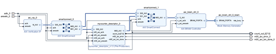
Block Diagram Setup
3. Navigate to the address editor and assign addresses to the custom DUT and the BRAM. In this example we assigned the BRAM to address 0 and the DUT to 0x4000_0000.
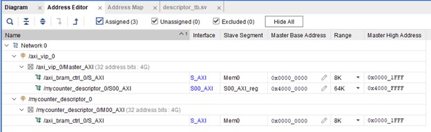
Address Editor
Go back to the block diagram and right-click on a blank spot in the design. Select Validate Design.
5. The next step is to create a wrapper file which turns the block diagram into HDL. To do this go to the Sources
and right-click on the source for your block diagram (the default name is design_1 or something similar). Select
Create HDL Wrapper and then Let Vivado manage wrapper and auto-update.
The next step is to create a testbench to ensure the custom AXI IP works as intended.
2.4. Testbench for a Master Custom DUT
The testbench for this advanced master counter DUT is similar to the testbench of the simpler DUT we previously created and follows all of the core concepts. The difference is that this advanced master DUT reads in the start value and counting mode from memory. It is important to remember this so you can first place these values directly into memory, and then send the DUT the command to read these values in before enabling the counter. Another thing important to keep straight are the addresses for writing to the memory directly(0000_0000 in this example with an offset of 200), and the address for writing to the DUT directly (4000_0000 in this example).
Follow the steps stated for creating a testbench for a simple counter. Make the appropriate address changes and update the logic to test all aspects of the advanced descriptor DUT.
A brief description of my testbench logic is stated below, the parentheses include the address that the command is sent to:
Write the start value and counting mode directly into memory (addr:0000_0204)
Initiate the counter to read the start value into the DUT (addr: 4000_0008)
Enable the counter (addr:4000_0000)
After a delay, initiate the DUT to send the current count out value to memory(4000_0008)
Disable counter (4000_0000)
Read count value that was sent previously directly from memory (0000_0200)
Write a new start value into memory, this time decrement mode (0000_0204)
Initiate the counter to read in the start value into the DUT (4000_0008)
Enable the counter
After a delay, disable the counter
Important
If you want to download the testbench file directly, go here.
2.5. Simulating the Master Custom DUT
This section is based on the Interpreting Simulation Waveforms For a Custom DUT earlier section. Please refer to that documentation for details.
Run the Behavioral Simulation
The waveform should have automatically opened. In the left column, there are some signals we want to add to the waveform. The first signal is
axi_vip_0, this will show the reads and writes that we initiate from the axi_vip in our testbench. In order to add a signal to the waveform, right click on the desired signal and choose Add to waveform. The next group of signals necessary to add to the waveform are for our custom DUT, in this example labeledmycounter_descriptor. This will show the writes written to the counter from the AXI VIP, as well as the commands the DUT performs to memory. And the last group of signals to add to the waveform isaxi_bram_ctrl_0. This will allow you to see the data stored in memory.
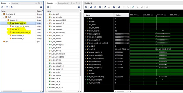
Add Desired Signals to Waveform
3. Now that we have added the necessary waveforms, in order to see the simulation run through our testbench properly we need to simulate for 3ms. To do this, make sure that the top toolbar is set to at least 3ms and then click the button highlighted in the photo below.

3ms Simulation time