1. FPGA Review and Emulation Overview
Important
This section is intended for FPGA and digital design beginners, although some intermediate concepts are briefly discussed.
1.1. A One Minute Introduction to FPGAs
This fantastic quick video from Charles Clayton outlines the very basics of an FPGA. If you do not know what an FPGA is, start here before moving on.
Still confused? Here is a more approachable example that may help:
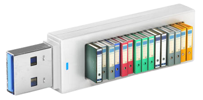
Imagine you had a box of USB sticks to sell, where each stick performs some task, whether it is counting from one to ten, transferring some songs to the hard drive, or even running another smaller computer. Because we hope to sell them, we should test every single stick (what we will refer to as a device under test) as much as possible for maximum compatibility to avoid any future errors or refunds. But, considering how many computers there are in the world, it is almost impossible to verify that every stick will work on every laptop or desktop aside from buying and testing on each one individually. The price for failure is high too, as a broken USB stick could potentially damage a user’s computer, leading to an expensive safety recall.
Now imagine if you had access to a special computer called an emulation evaluation board. From the outside, it is like any other computer, as the board also has USB, Ethernet, and other standard peripherals. However, at the heart of the board is what is known as an FPGA, a special kind of chip that can replicate/emulate every other computer in existence. Although a little clunky and hard to use, this FPGA means that you can now rest assured knowing that your USB sticks can be fully tested on every possible configuration before being sold. Not to mention, the board only needs to be set up once as an emulation environment before you’re able to easily swap in and out DUTs for testing. Not bad, right?
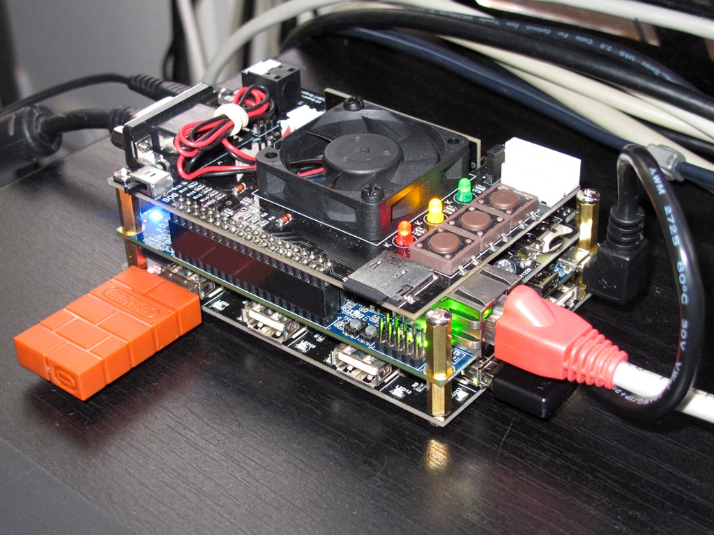
A MiSTer board with Cyclone V FPGA
Ready for a (slightly) technical deep dive? Read on for more details.
1.2. What is an FPGA anyways?
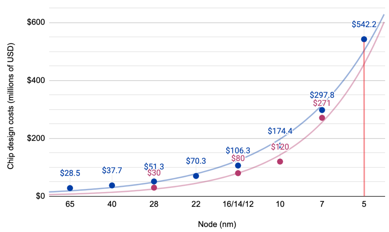
In 2020, Apple unveiled their newest computer chip, the M1, as the first 5nm processor for their range of Macintosh computers. As their very first in-house designed system on a chip, or SoC, the process of creating the M1 and other competitors like the Qualcomm Snapdragon 888 was very expensive, with costs reaching into the hundreds of millions of US dollars.
As an SoC iterates through each design and manufacturing step, the harder (and more expensive) it becomes to correct any errors. Think of a nightmare scenario where a manufacturer is forced to recall every single smartphone and computer due to a fatal bug with the CPU that was never caught (this happened to Intel and their Pentium processors in 1994!) This is where an FPGA becomes extremely useful.
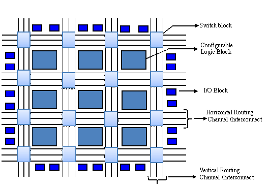
Field programmable gate arrays or FPGAs are integrated circuits (a set of circuits layered within semiconductor material like silicon, also known as chips) designed to be configured by a customer or designer after manufacturing. With FPGAs, a designer can program features, adapt to environment and regulatory changes, and reconfigure hardware even in the field - hence the term field programmable. An FPGA contains programmable logic elements (LEs) that either act as basic logic gates or connect to perform complex actions as logic blocks. From a top-level perspective, FPGAs consist mostly of configurable memory, high speed I/O, logic blocks, and routing.
While SoCs like the Snapdragon 888 and other ICs are not intended to be physically changed after manufacturing, FPGAs allow for design flexibility and provides the opportunity to change how sections in a system work without introducing subsequent cost, delays, or design risk. For example, because FPGAs excel in processing digital signals quickly, one common application is machine vision. An FPGA projecting a back-up camera onto the rear-view mirror of a self-driving car can be modified to reduce latency and comply with new government standards simply through a software update. Conversely, this flexibility is almost impossible with a microprocessor, as any drastic changes would ultimately result in a complete redesign.
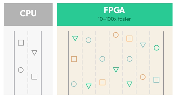
This optimized behavior is possible due to one key point – FPGAs operate in parallel. Normally, a processor must load in instructions in a linear fashion, even for simple tasks such as multiplying or shifting bits. Each instruction must be evaluated in order before the CPU can move onto the next one. This is fine under normal use, but in real-time applications where latency must be as low as possible, having to wait for the AC to activate before the brake pedal can be used is unacceptable. In contrast, an FPGA can execute multiple complex operations simultaneously — with a 10-element matrix, a designer can implement 10 signal/data pipelines to use in parallel. While a microprocessor has sequential processing, an FPGA’s concurrent processing allows it to achieve better optimization and a more deterministic latency than even a processor running an RTOS.
In more nuanced terms, the flexibility from an FPGA allows a designer to decide which operations occur at any given clock cycle. Even though FPGAs are clocked much slower than CPUs (100 MHz vs. up to 4 to 5 GHz), given the right design, FPGAs can become much more optimal than even the fastest CPUs. For example, instead of only being able to multiply two numbers at every cycle with a CPU, a designer can use all 10 pipelines to multiply 20 numbers for every single cycle - 1/10th the time it would take with a traditional CPU, assuming that the CPU is never interrupted by another instruction. Because an FPGA has very high determinism (in that we know exactly when each instruction will execute), we can rest easy knowing that the FPGA will never be unintentionally interrupted and continue to perform at a consistently high threshold.
Important
If you are coming from a traditional programming background, this is an especially crucial point. You are most likely accustomed to coding in sequential order, so always consider concurrency when working with FPGAs!
1.3. What’s Inside an FPGA?
While a software engineer writes linear high-level code to become compiled into low-level assembly instructions, a hardware designer does not have a compiler; instead, they manipulate much lower-level discrete digital components like LUTs, registers, etc. Again, this is important to remember moving forward — while programmers write software code, FPGA designers ‘code’ physical hardware present on the FPGA itself.
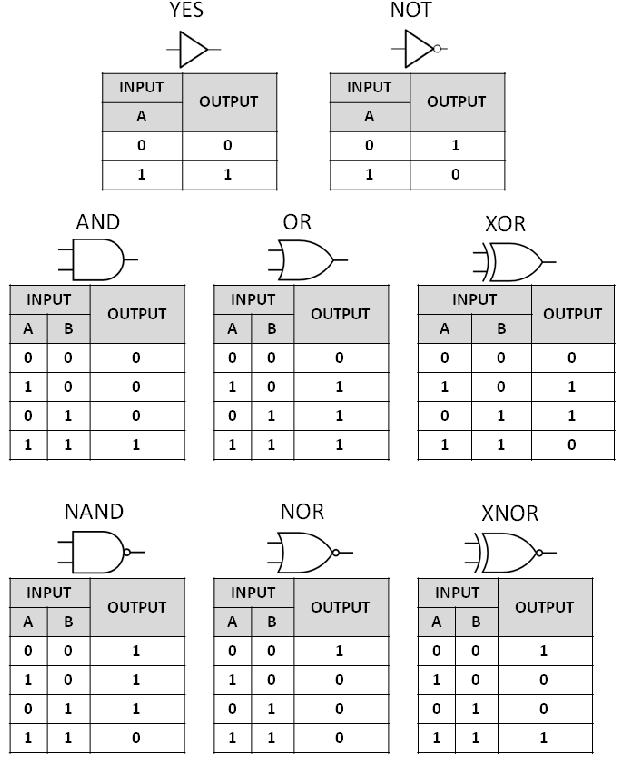
The smallest component on an FPGA is the simple logic gate. Of course, discrete logic gates do not physically exist inside an FPGA — instead, FPGAs calculate Boolean algebra using look up tables (LUTs) as truth tables, where each LUT can calculate any Boolean algebra equation based on the number of inputs. A typical FPGA will have thousands of three, four, and five-input LUTs. More about Boolean algebra and logic gates here.
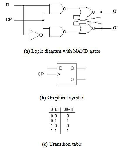
By combining multiple logic gates together, we can create truth tables that achieve more complicated functions. One of the most common examples is a D flip-flop, a logic component that changes the output Q based on the input D. The FF stores the current value on the D data line, essentially acting as a basic memory cell. FFs use sequential or registered logic, meaning that it operates based on the regular transitions of a clock, driven by the clock input line (>). FFs register data from D to Q on a clock’s rising (or falling) edge, or when the clock transitions from 0 to 1 (or 1 to 0). With multiple flip-flops (or registers in this case) all acting as data storage elements, they collectively store the current state of the entire FPGA, including counters, state machines, and evaluations of other components. If an FPGA only had LUTs without any FFs, the FPGA would have no memory, forced to immediately evaluate all changes on any inputs and preventing any saved programs from working (meaning that our multiplication example from before would no longer function).
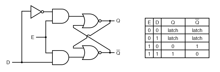
In a similar manner, a gated D latch is a simpler non-clocked flip-flop that is also used to store state information. A D flip-flop uses a clock signal to transfer data, while a latch simply checks an E enable input line. As before, input D is the data input line, containing the value to transfer to output Q (or Q bar, the opposite of Q). Q only receives the value on D when Enable is HIGH or 1 — when E is 0, output Q is considered ‘latched’ and will not change regardless of input D.
Note
Latches are often created unintentionally from incomplete assignments, so beginners are not advised to use them until they have significant FPGA debugging experience.
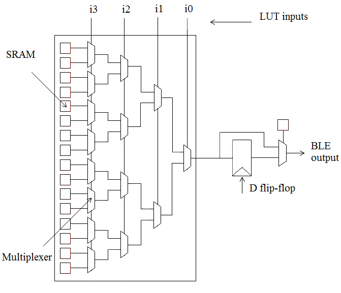
From an overarching perspective, an n-bit LUT is implemented as a \(2^{n} \times 1\) memory component. In other words, \(2^{n}\) SRAM latches hold the value of each LUT input combination, creating a larger general purpose truth table. Each latch is controlled by a \(2^{n} \times 1\) multiplexer, or mux, which is a simple logic component that chooses which of its multiple inputs to transfer to its output line. LUT inputs into the mux control determine which latch values are passed to output Q. For example, 16 latches store multiple values in memory and feed into a 16 by 1 mux. The mux also receives control inputs that determine which latch is pushed to the output.
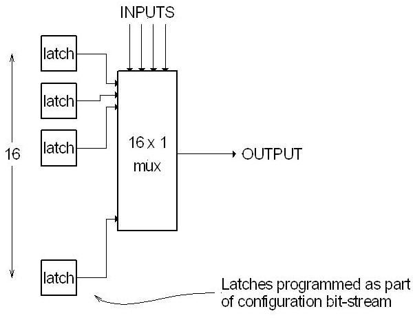
Abstracted block diagram of a look-up table
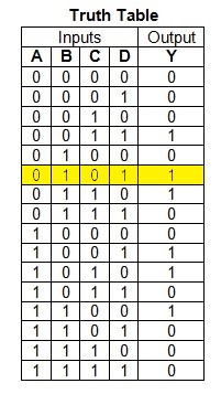
For example, given a 4-input truth table with 16 rows, for the input ABCD = 0101, the output Y will be 1 7.

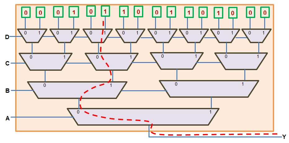
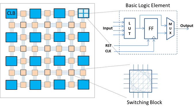
A flip-flop then stores the LUT’s output. One last multiplexer decides, based on the given configuration, whether the output receives the value from the flip-flop or directly from the LUT itself. As a whole, all components make up a single configurable logic block (CLB). Like the introductory video, these logic blocks are routed togther using switching blocks to finally make up the entire FPGA floorplan 8.
1.4. The Basics of Hardware Emulation and HDLs
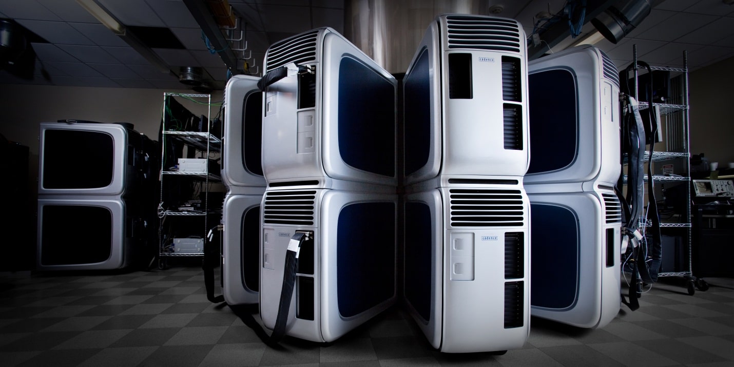
As we have discussed at length, FPGAs provide an unparalleled combination of performance and flexibility that rivals even the most expensive processors (of course, industry-grade FPGAs cost quite a bit too). This reprogrammability allows FPGAs to excel at one of their most interesting applications — hardware emulation or the method of copying the behavior of another hardware sample. Referring to our Apple M1/Qualcomm 888 example, instead of manufacturing new designs on the assumption that they will work 100% of the time, most if not all semiconductor companies first use FPGAs to emulate their chips. Hardware emulation allows these manufacturers to debug their designs in simulated but realistic conditions before undertaking the extreme cost of mass fabrication. By chaining multiple FPGAs together (sometimes up to the scale of entire rooms for one chip alone), these companies are able to logically simulate even the most complex integrated circuits in real time, testing both hardware performance and software compatibility. Modern GPUs and CPUs have billions of transistors, so ultimately hardware emulation is and will continue to be an essential part in the semiconductor industry.
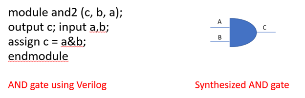
Hardware emulation is achieved through a number of steps. First, the design is created from HDL code, also known as a hardware description language. Similar to traditional programming languages like C or Python, an HDL like Verilog or VHDL instantiates the FPGA’s physical hardware using digital code. HDLs execute instructions in parallel, while software languages operate in sequential order. Designs are then synthesized, wherein the human-understandable code is converted in a netlist of connected logic gates or flip-flops. Essentially, synthesis acts the same as compiling software code to machine assembly code.
Place and route (P&R), or implementation, is a set of multiple procedures in which the list of nets is physically placed and mapped to the FPGA’s resources. Implementation creates a roadmap where each element can be placed onto the FPGA chip. At the end, the software will output a bitstream that designers can program onto the FPGA for further testing. Both synthesis and implementation are typically done with first-party software, although synthesis can be completed with third-party alternatives.
Finally, the tasks of simulation and verification provide useful debugging methods along the entire development process. Verification is a multi-stage procedure from writing a testbench or set of tests in HDL code that checks the design against a given specification to testing for timing concerns. Behavioral simulation is one aspect of verification that simulates an environment based on the testbench and outputs relevant signal waveforms. Do not worry if you have little experience with reading waveforms or using an oscilloscope, as we will be explaining our simulation tests in every example project we provide using Vivado’s ModelSim. This article will not go into SystemVerilog and UVM, as that is outside the scope of this entire project.
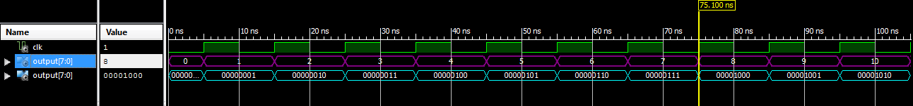
Simulating an 8-bit binary counter
Of course, going through the entire process from synthesis to bitstream for every single hardware component is time-consuming, especially if you are repeatedly working with the same FPGA. It would more efficient and easier to first create the infrastructure first in the form of an emulation environment. This would include peripherals like the board memory or PCIe pinout, which never change between designs. After all, if you end up working with the same board, why start from scratch for every project? A premade environment allows us to get a running start for every future project onwards, which is why setting up such an environment is our first example project.
Note
Don’t worry if you don’t have access to a physical FPGA board — 90% of design work is done in simulation anyways!
After the environment is completed, we will continue to guide you through creating and simulating a device under test (DUT), letting you emulate everything from a simple counter to a complex SoC.
Important
Jump here to get started with your environment. Otherwise, continue to the next page for a deeper introduction into the hardware.
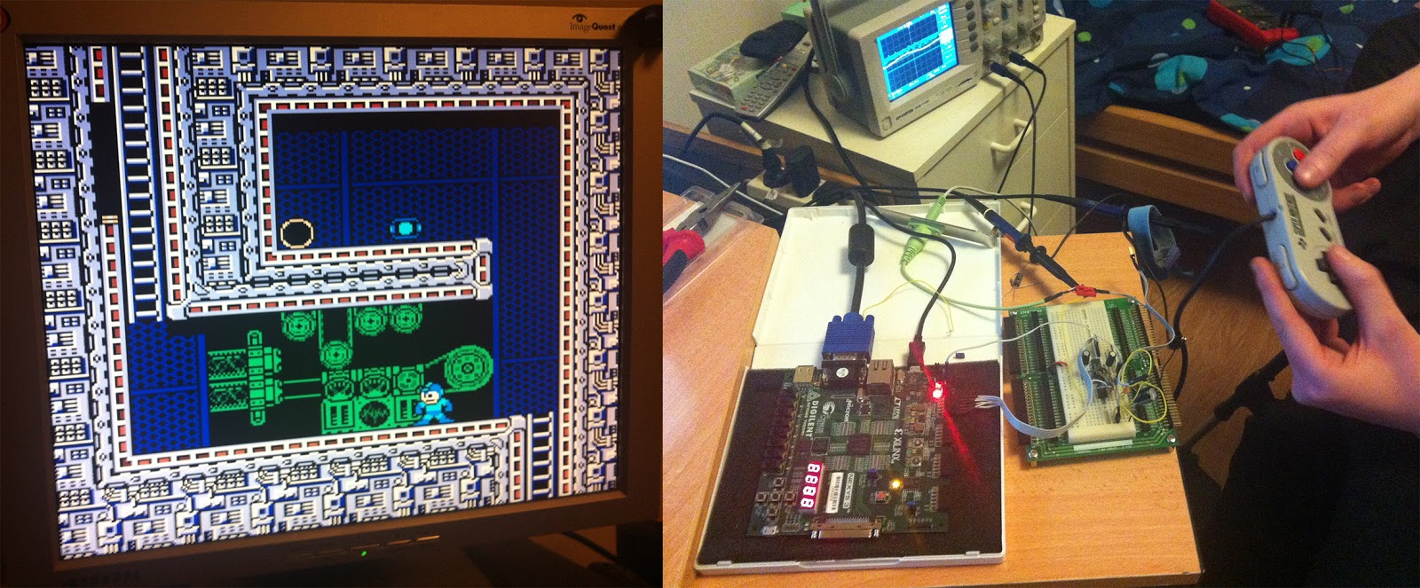
What is a real-world example of hardware emulation? One interesting application that has evolved in the last few years is the MiSTer project, an open-source design that emulates old video game consoles using nothing more than a small FPGA board. Using the same principles as software emulation, the MiSTer project emulates multiple reversed-engineered consoles on a single Altera Cyclone FPGA, opening the opportunity for a home arcade at a fraction of the price. Instead of paying hundreds of dollars for a new and working Nintendo Famicom Disk System, which was never released in the West, or use software emulation to run code in a similar fashion, the FPGA board can instead emulate the console hardware itself and play every game that was ever released with the same level of performance and compatibility. Of course, since FPGAs are flexible, an FPGA can reconfigure itself through LUTs to emulate other hardware. This means that different console cores from Atari to Pac-Man can be swapped out at any time, again illustrating the versatility of FPGAs and serving as a good example for our emulation environment project. By building up the proper infrastructure, it would become easy in the future to swap in different DUTs like the MiSTer cores for testing and debugging, similar to standard industry practices in the semiconductor field. All without even touching the original hardware.
1.5. Quick Definitions and Acronyms
- ICIntegrated Circuit
Collection of electronic components on a single unit, typically made from silicon, also known as a chip.
- FPGAField Programmable Gate Array
ICs designed to be configurable by engineer after manufacturing.
- ASICApplication Specific Integrated Circuit
Highly specialized ICs dedicated to one specific application.
- SoCSystem on a Chip
IC that hosts an entire computer system by itself.
- P&RPlace and Route
Process by which logic components are placed onto an FPGA and connected/routed together.
- DUTDevice Under Test
Any electronic part currently being tested, through emulation in our case.
- IPIntellectual Property
Commonly used electronic parts abstracted as logic blocks, provided by external companies (not the same as a patent).
- AXIAdvanced eXtensible Interface
Communication standard that allows chip components to send signals to each other.
- MIGMemory Interface Generator
Xilinx IP that allows an FPGA to read/write into DDR memory.
- DDR SDRAMDouble Data Rate Synchronous Dynamic Random-Access Memory
Volatile memory IC typically used to store information that is lost when power is lost, common interfaces are DDR3 and DDR4.
- PCIePeripheral Component Interconnect Express
Communication network that allows an FPGA to control peripherals/communicate with a host PC.
- TLPTransaction Layer Packets
Data payloads that peripherals send through the PCIe bus.
- DMADirect Memory Access
Xilinx IP that allows AXI peripherals to directly access memory without the help of the processor.
- ROMRead Only Memory
Flash memory that cannot be modified afterwards.
1.6. References
- 1
The example FPGA ADC/DAC board used.
- 2
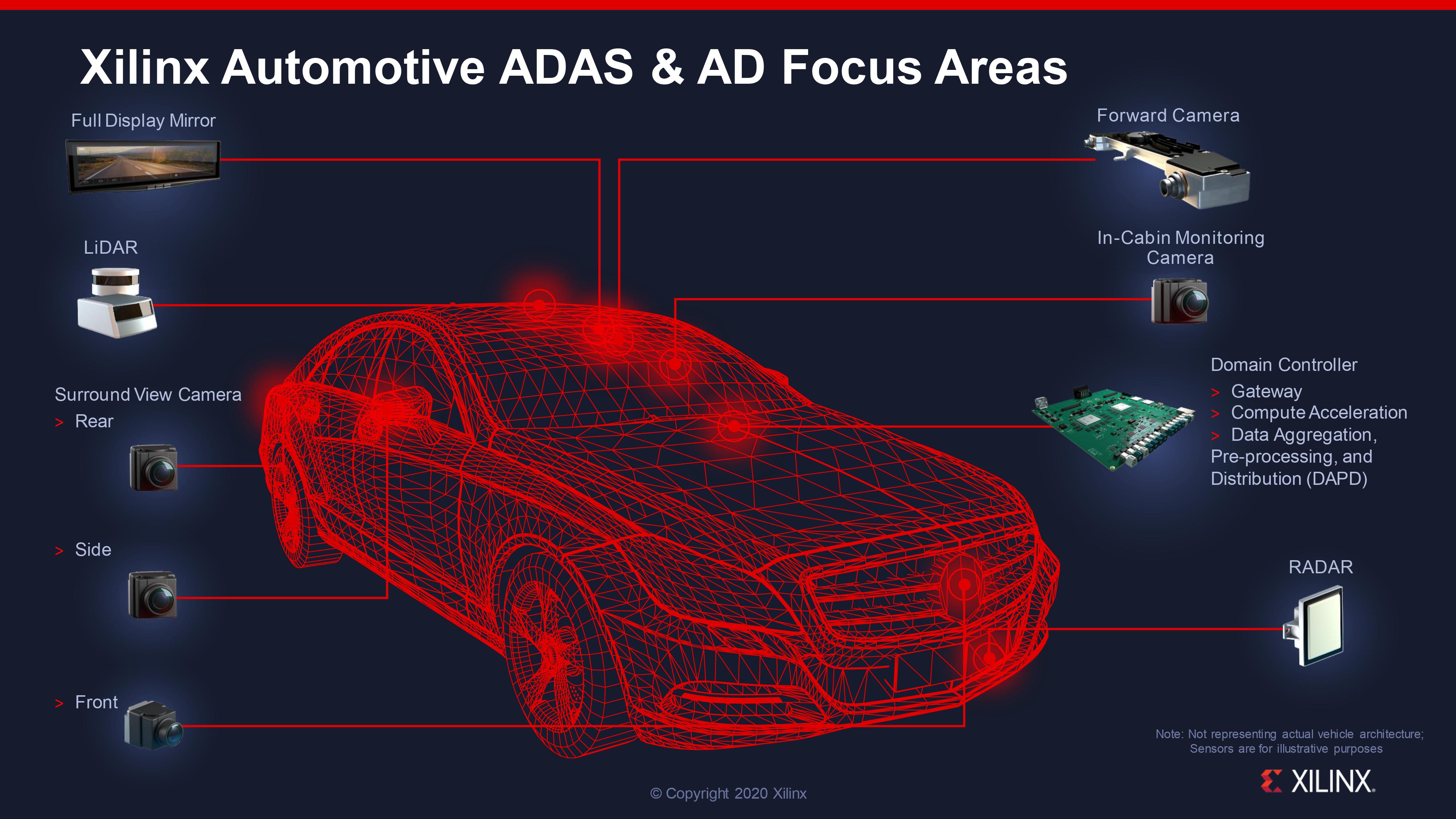
Xilinx’s automotive system is discussed in this press release.
- 3
More about FPGA computational performance can be found in this article.
- 4
From Abels, S. G., & Khisamutdinov, E. F. (2015). Nucleic Acid Computing and its Potential to Transform Silicon-Based Technology. DNA and RNA Nanotechnology, 1(open-issue), 13-22.
- 5
More about flip flops and their diagrams are here.
- 6
From Abdel-Lattif, G. Y., Rehan, S. E., & Abdel-Fattah, A. F. I. (2012). OPTIMIZED SINGLE-ELECTRON NAND-BASED D-LATCH/FLIP-FLOP. The Mediterranean Journal of Electronics and Communications, 8(4).
- 7
More about LUTs here.
- 8
FPGA floorplan from this info page.
- 9
More about NVIDIA’s emulation lab in this blog post.
- 10
Details about the FPGA design flow here.
- 11
Venugopal, N., Shobana, V., & Manimegalai, R. (2014, January). Analysis of optimization techniques in FPGA placement. In 2014 International Conference on Computer Communication and Informatics (pp. 1-5). IEEE.
- 12
More about the NES FPGA project here.