2. AXI Protocol Overview
2.1. The AXI Protocol
When building your first block diagram or reading the documentation of Xilinx’s IP cores, you may notice one thing in common – they all use the AXI protocol. This article will provide a brief explanation about what AXI is and how it functions.
The Advanced eXtensible Interface, or AXI, protocol is a royalty-free communication standard developed by ARM, a prolific system-on-chip (SoC) company, as part of the AMBA (Advanced Microcontroller Bus Architecture) standard. You can find more information about AMBA and its other protocols (such as AHB or APB) here.
Essentially, the AXI protocol outlines the process by which on-chip components can communicate with each other using signals, usually involving a master and slave device. By standardizing this protocol, we can ensure every peripheral and IP core present on an FPGA will be able to talk to each other, creating a cohesive system (rather than a scattered collection of cores).
There are three types of AXI4 interfaces (defined by AMBA 4.0):
Full AXI4 - High-performance communication, using memory-mapped addresses (more here).
AXI-Lite - Lightweight and simple memory-mapped interface, used for single transaction communication.
AXI4-Stream - ‘Direct’ device communication, removing the need for addresses and allowing for maximum data transfer.
For the remainder of this article and throughout our projects, we will mainly focus on Full AXI4 for the best performance-cost ratio.
2.2. AXI Reads and Writes
AXI4 allows for multiple data transfers over a single request, allowing for greater data bandwidth in the scenario where large amounts of data must be transferred to/from specific addresses. This multi-transfer request is also known as a burst.
All AXI communication is with respect to memory addresses, which each have a specific purpose defined by the RTL and top module.
Three burst types are supported - FIXED, INCR, and WRAP. Each one alters the transfer address in a specific way, allowing for optimal transfers in different situations. For example, a FIXED burst sets every beat to have the same address, which is useful for memory transfers from the same repeated location.
In general, burst addressing specifies where each read or write should be performed in which addresses. Each burst type is as follows 1:

AXI Bursts
AXI4-Lite has no burst protocol (only sending one piece of data at a time) while AXI4-Stream acts as a single unidirectional channel for unlimited data flow between a master and slave, removing the need for addresses.
2.3. AXI4 Connections and Channels
In its most basic configuration, the AXI protocol connects and facilitates communication between one master and one slave device. As expected, the master initiates and drives data requests, while the slave responds accordingly. This communication, or transactions as we will now refer to, occurs over multiple channels, each one dedicated to a specific purpose.

AXI Handshake Protocol
The sender must always assert a VALID signal before the receiver and keep it HIGH until the handshake is completed. By using handshakes, the speed and regularity of any data transfer can be controlled.
There are five channels, each one transmitting a data payload in one direction. Each channel implements a handshake mechanism, wherein the sender drives a VALID signal when it has prepared the payload for delivery and the receiver drives a READY signal in response when it is ready to receive the data. The data transfer is also known as a beat.
The five AXI4 channels are as follows:
Write Address channel (AW): Provides address where data should be written (
AWADDR)
Can also specify burst size (
AWSIZE), beats per burst (AWLEN+ 1), burst type (AWBURST), etc.
AWVALID(Master to Slave) andAWREADY(Slave to Master)
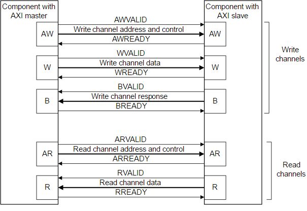
Write Data channel (W): The actual data sent (
WDATA)
Can also specify data and beat ID
Sender will always assert a finished transfer when done (
WLAST)
WVALID(Master to Slave) andWREADY(Slave to Master)
Write Response channel (B): Status of write (
BRESP)
BVALID(Slave to Master) andBREADY(Master to Slave)
Read Address channel (AR): Provides address where data should be read from (
ARADDR)
Can also specify burst size (
ARSIZE), beats per burst (ARLEN+ 1), burst type (ARBURST), etc.
ARVALID(Master to Slave) andARREADY(Slave to Master)
Read Data channel (R): The actual data sent back
Can also send back status (
RRESP), data ID, etc.Sender will always assert a finished transfer when done (
RLAST)
RVALID(Slave to Master) andRREADY(Master to Slave)
Here is an example of a typical read/write AXI transaction.
To write, the master first provides the address (0x0) to write to, as well as the data specifications (4 beats of 4 bytes each, data type of INCR). Both the master and slave then exchange a handshake for verification.
The master then prepares and writes the actual data payload to send over the channel (0x10, 0x11 0x12, and 0x13), again using a handshake to verify the transfer. The master will signal the end of the payload to the slave using
WLAST.The slave responds with a status of the write and whether it was successful or a failure (all OKAY in this case) and finishes the entire transaction with another handshake.

A typical AXI Write transaction
To read, the master first provides the first address to read from (0x0), as well as the data specifications (4 beats of 4 bytes each, data type of INCR). The usual handshake occurs.
The slave then provides the actual data payload, as well as the status of each beat (all beats are OKAY). The slave will signal the end of the payload to the master using
RLAST. As we can see, what was written to the specified addresses was the same as what was read back.

A typical AXI Read transaction
We can also get an idea about what an AXI read and write cycle would look like in simulation through the
7 Series MIG documentation (UG586). As we can see, an AXI write consists of a command cycle
(define address and burst length), data cycle (putting the data payload over the channel), and a response
cycle (checking if the data was received). The master defines the payload specifications and writes the
actual data payload (5a5aa5a5 at address 00000000). The slave toggles s_axi_bvalid, exchanging
a handshake that signifies the transfer was successful.
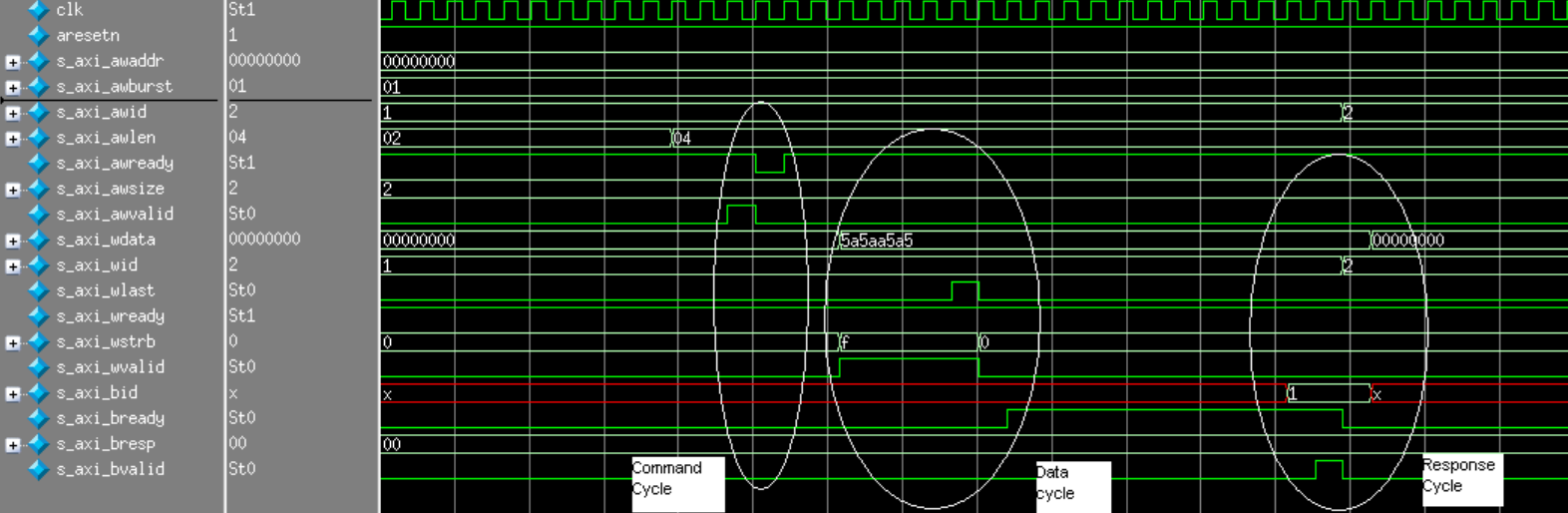
AXI Write Cycle in Simulation
Subsequently, an AXI read consists of a read command cycle (again, defining the address to read from, burst
length, etc.) and a read data cycle (receiving the data from the requested address). The master specifies
the address (00000000) and other payload specs, receives the data payload from the slave (5a5aa5a5),
and exchanges a final handshake by toggling s_axi_rlast to complete the transfer.
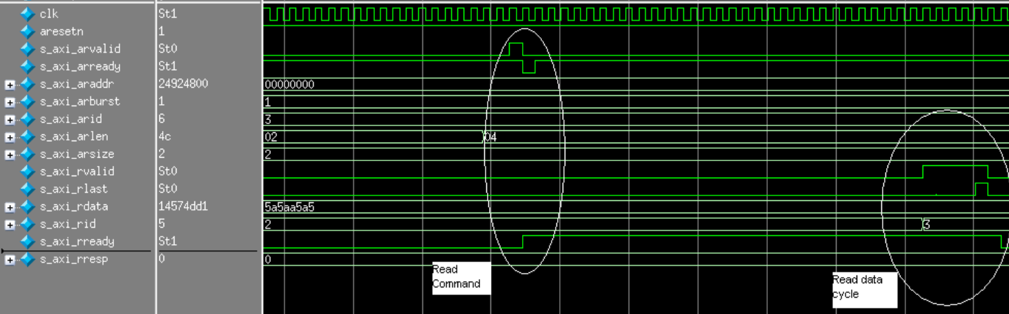
AXI Read Cycle in Simulation
2.4. AXI Interconnect vs. SmartConnect
AXI is a very flexible standard in that it only outlines the interface itself, never requiring a designer to memorize multiple configurations for every scenario. This characteristic is exemplified with the introduction of the AXI Interconnect IP.
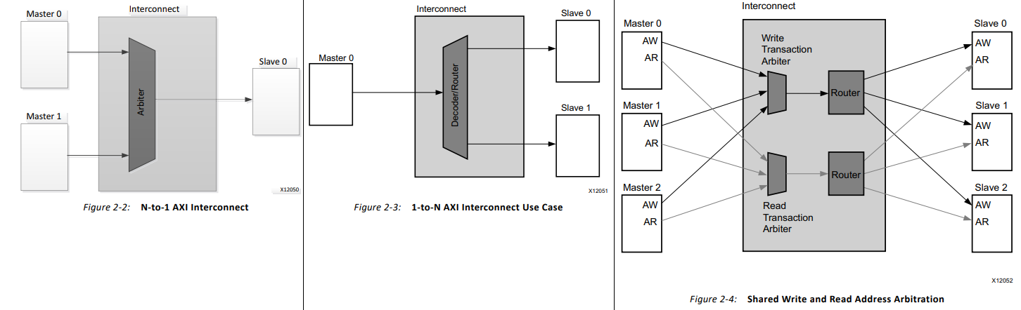
The AXI Interconnect IP is similar to an operating system in that both mediate data and resource transactions between two independent entities. The Interconnect IP is made up of a combination of arbiters, decoders/routers, multiplexers, and other logic elements that seamlessly adapts to any AXI system, whether it be a multi-master system connected to one slave, a multi-slave system connected to one master, or multiple masters connected to multiple slaves (up to 16 each).
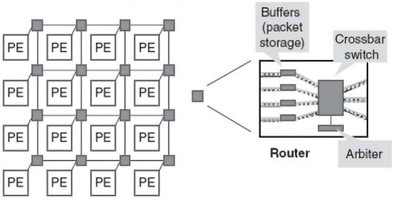
The AXI Interconnect is also known as a network-on-chip (NoC). There are many technical details about NoCs that we will not go into here, such as topology and routing strategies, but the only characteristic to keep in mind is that NoCs use packets, not wires, to route data from the source to the destination. While traditional Verilog instantiates connections between modules as wires and sends electrical signals as communication, NoCs like the Interconnect or SmartConnect utilize the AXI protocol to route signals and data payloads from the master to the appropriate slave device. The NoC architecture has multiple routers connnected by wires or links with an array of processing elements or PEs built on a mesh topology. This creates a scalable architecure that has a higher bandwidth than connecting each module individually.
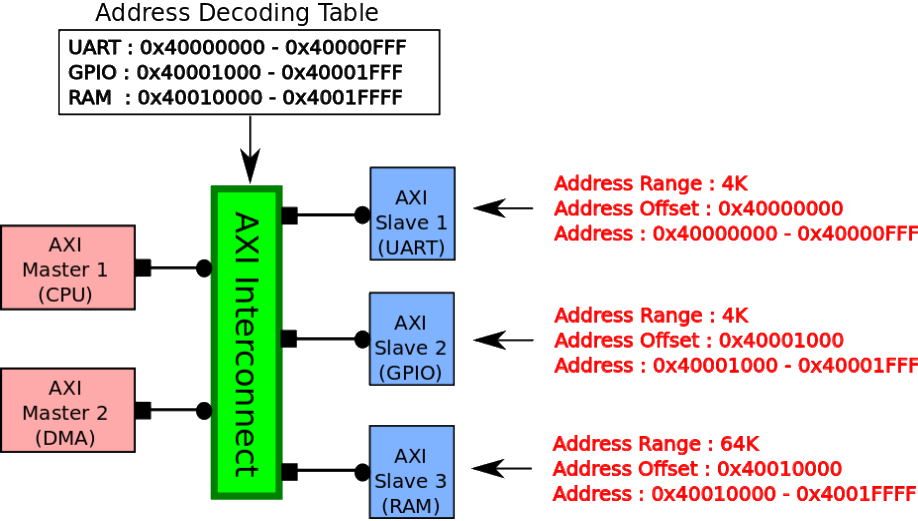
For a multi-master/slave system, the Interconnect will contain multiple arbiters and routers so that each write and read channel has a dedicated connection between masters and slaves — by doing this, both reads and writes can occur simultaneously. This is also known as an AXI Crossbar core. A typical Interconnect transaction would occur in this manner:
As always, the master first provides the address for a write transfer onto the AW channel. The write transaction arbiter decides which master can monopolize the Interconnect Write channel and sends the master’s address to the router.
Using a preallocated address decoding table, the router then decodes the given address and selects the proper slave to write the address to. The typical AXI write transaction then commences, with an Interconnect multiplexer mediating a data transfer between master and slave.
At the same time, another master can provide a different address to read from on the AR channel. The read transaction arbiter can also decide which master monopolizes the Interconnect Read channel, sending that master’s address to a different router.
This second router also decodes the given address and selects either the same or a different slave to read from. An AXI read transaction then starts with another Interconnect multiplexer as a mediator.
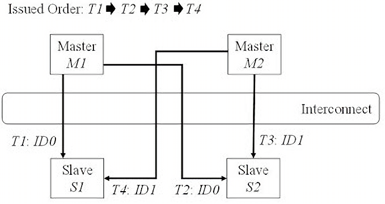
The Interconnect IP works on a round-robin basis, wherein the read and write channel will alternate for access if multiple masters are trying to write to/read from the same slave. Since the DDR protocol allocates a few clock cycles between reads and writes, the IP cannot immediately switch channels. Because slaves can queue multiple transactions and this round-robin schedule allows for out of order transfers (a slave device can respond to a master whenever), a deadlock risk emerges. Deadlock is a scenario where a transfer #1 cannot fully complete while transfer #2 is running. To finish, #2 requires transfer #1 to complete first, creating an endless loop that is never resolved. You can read more about the Dining Philosophers Problem here.
From the Xilinx’s Interconnect Documentation 2, we can see how a deadlock situation can form:
Master M1 reads from Slave device S1 using ID0.
Master M1 then reads from Slave device S2 using the same ID thread ID0.
Master M2 then reads from Slave device S2 with a different ID ID1.
Master M2 then reads from Slave device S1 using the same ID thread ID1.
Slave S1 responds to Master M2 first. It is allowed to respond to M2 before M1 first, since the two Masters have different IDs. However, the AXI Crossbar cannot pass the response to M2 because Master M2 must first receive its response from Slave S2.
Slave S2 responds to Master M1 first without re-ordering. But the AXI Crossbar cannot pass the response to Master M1 because M1 must first receive its response from Slave S1, resulting in a deadlock situation.
Helpfully, the AXI Interconnect IP already resolves this concern by mandating the “Single Slave per ID” rule, where generally only one master device can talk to any slave at any given time. With this in-order rule, the Read transaction in step 2 from M1 to S2 is stalled until S1 completes its response to M1. Similarly, the transaction between M2 and S1 in step 4 is stalled until S2 completes its response to M2. This is important to keep in mind as the AXI protocol itself has no in-order check between Read and Write transactions, meaning that deadlock can occur elsewhere, especially when combining multiple Interconnects and SmartConnects together.
The Interconnect also can update AXI3 interfaces to AXI4, perform bus-width conversion, use input/output FIFOs and register slices to break down timing paths, and convert between different clock domains. Simply put, the Interconnect IP is a versatile core that allows a designer to utilize the AXI protocol to its fullest extent without diving deep into the technical minutiae.
However, at the time of writing, the AXI Interconnect v2.1 core has been obsoleted by the new AXI SmartConnect IP. The SmartConnect operates on the same AXI4 principles of the Interconnect IP, providing similar performance with better optimization and a more streamlined experience. The AXI SmartConnect supports wider addressing and multi-threaded traffic along with a myriad of other benefits, so while Xilinx notes that pre-existing designs with the Interconnect v2.1 core do not need to upgrade, new designs are recommended to use the SmartConnect core moving forward. As such, our example designs will (almost) always use the SmartConnect IP as opposed to the older Interconnect. For more information, read the SmartConnect v1.0 documentation (PG247).
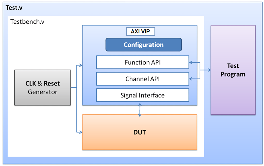
2.5. AXI Verification IP
With some of our example designs, we have chosen to use the AXI Verification IP or AXI VIP as a test DUT. The VIP, which is
provided by Xilinx, is a useful AXI4 core that allows us to debug our block designs and verify for expected behavior. It is the successor
to the now obsolete AXI Bus Functional Model or BFM and all new designs will use the VIP moving forward, as the BFM is no longer available.
The VIP can be dropped into any design and simulate a master, slave, and pass-through device (connecting a Slave to Master).
It has one (optional) active LOW reset aresetn which is synchronous to aclk. This IP is mainly for simulation and is
not synthesized. We will be using the VIP to verify data transactions in simulation and overall it is a good introductory method
for catching errors in any custom AXI IPs (although the VIP suite is prone to missing some background transfer errors).
While setting up the emulation environment and custom DUTs, we will be using the VIP to monitor and generate AXI transactions, as well
as check for protocol compliance.
2.6. References
- 1
AXI example images used from Wikimedia Commons and the AXI Article.
- 2(1,2)
AXI Interconnect documentation from Xilinx here.
- 3
From Sudeep Pasricha (Colorado State), Nikil Dutt (UC Irvine) “On-Chip Communication Architectures”, Morgan Kaufmann, 2008
- 4
The example of Interconnect Addressing from Mohammadsadegh Sadri, PhD, can be found in this post.
- 5
From Chou, H. M., Chen, Y. C., Yang, K. H., Tsao, J., Chang, S. C., Jone, W. B., & Chen, T. F. (2015). High-performance deadlock-free id assignment for advanced interconnect protocols. IEEE Transactions on Very Large Scale Integration (VLSI) Systems, 24(3), 1169-1173.
- 6
Read more about the SmartConnect IP in this white paper.
- 7
More about AXI BFM architecure here (modified image).