1. MIG 7 Series IP Overview
The MIG 7 Series IP is a ubiquitous core that is compatible with all 7 Series FPGAs, adding easy memory management into any design. For this article, we will discuss using the MIG with both a Kintex-7 and Virtex-7 board, such as the KC705 and VC707 respectively.
1.1. Customizing the IP
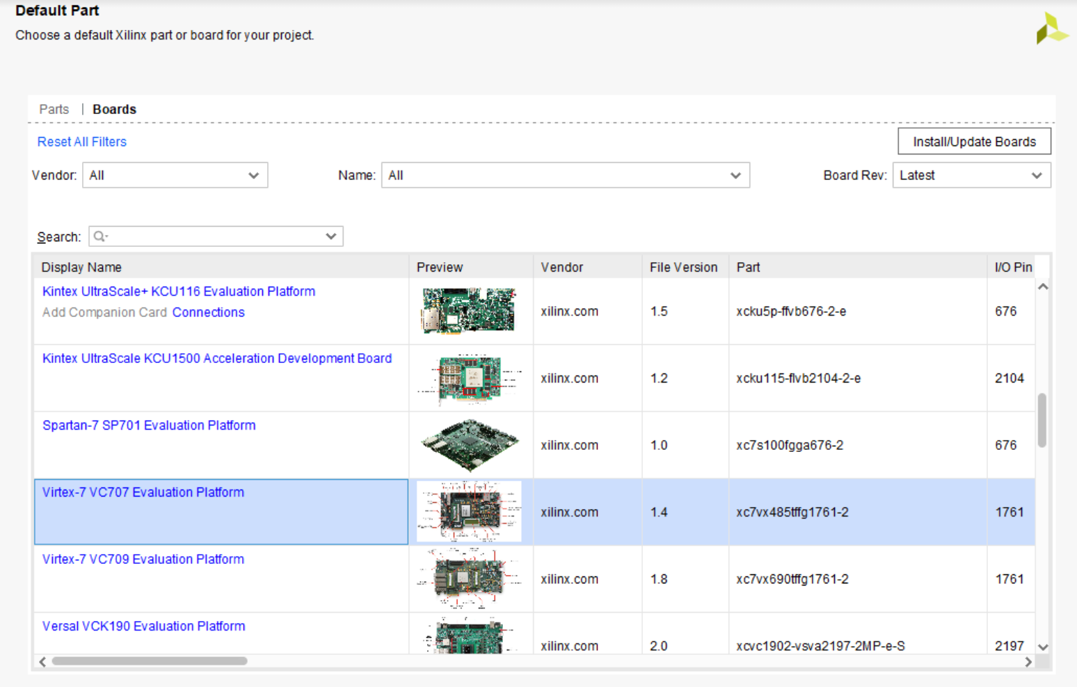
If using a board, be sure to select it as the project’s default part before moving on. A good board to start with is the VC707, as it has ample computational power, DDR3 memory, and a PCIe interface, as well as other peripherals.
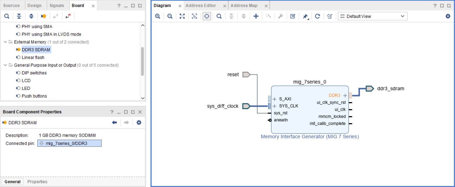
Create a new block diagram (BD) and use the IP catalog to add a new IP to the BD - in this case, the “Memory Interface Generator (MIG 7 Series)” core. If using a board, a prepackaged MIG may be available. We can customize it by double clicking it.
Important
Unless mentioned otherwise, leave all values default.
Make sure the AXI4 interface is enabled and select DDR3 SDRAM.
The desired clock period must be between 2500 and 3300ps. For now, use 2500ps (400 MHz), as this is the speed of the actual physical DDR3 RAM transactions.
Make sure the PHY to Controller Clock Ratio is 4:1 (ensuring that the physical DDR RAM will operate at 400 MHz, but the controller stays at 100 MHz i.e., ui_clk = 100 MHz).
For Kintex-7, select 8 bits as the Data Width for each address in memory. Also check that the number of Bank Machines used for managing DDR banks is set to 4. For Virtex-7, set the Data Width to 64 bits to account for the larger data bandwidth.
At the bottom of the Controller 0 screen, make sure the memory details match
1 GB, x8, row:14, col:10, bank:3, data bits per strobe:8, with data mask, single rank, 1.5VThe AXI Address Width is equal to the bank + row + column width = 3 + 14 + 10 = 27 bits wide.
Leave the AXI ID Width at 4, as we will not use this.
Select the Input Clock Period for PLL input clock (CLKIN) at 5000ps for 200 MHz, so that we can use the input clock as the reference clock, which must be 200 MHz. Deselect any additional clocks.
Make sure the Memory Address Mapping Selection is set to the default configuration of Bank/Row/Column.
Use No Buffer for the System Clock and Use System Clock for the Reference Clock, allowing us to use the system clock to also drive the reference clock at 200 MHz.
Choose active HIGH for the System Reset Polarity.
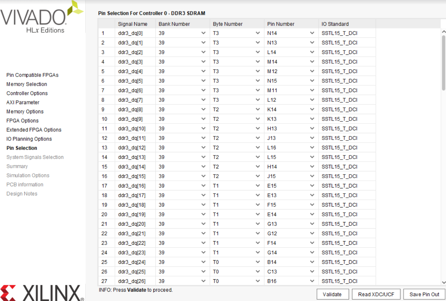
Import and validate the Pin Configuration file. Boards will come with preset constraints. For example, the VC707’s pins are as such:
After specifying the pinout, leave all system signals to their default values on the final page.
Accept the T&C, generate, and save.
1.2. Simulating the Example Design
Right click the IP core under the Sources menu and click Open IP Example Design, which will create a new example Vivado project, connecting the generated MIG to a Traffic Generator IP using AXI4.
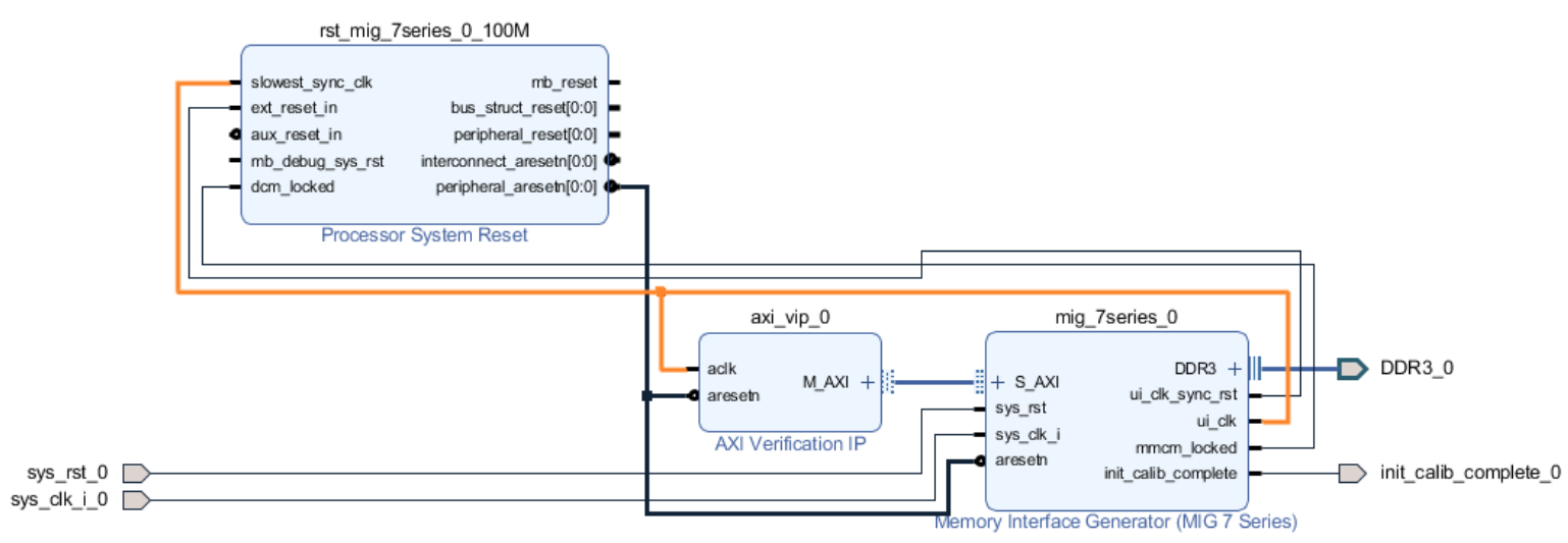
After running synthesis and implementation, your schematic should look similar to this:
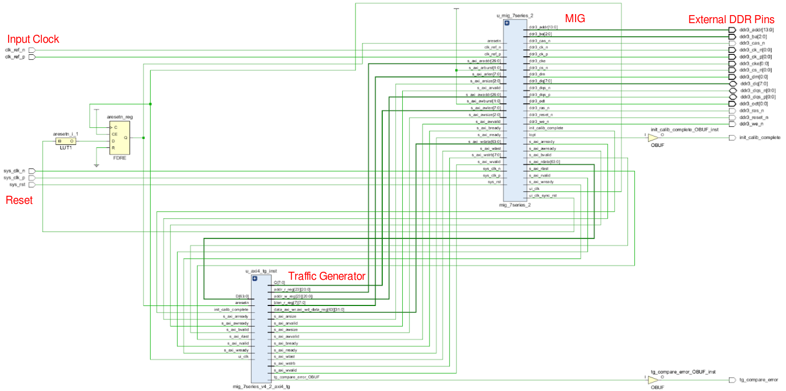
Looking at the 7 Series MIG documentation (UG586), we can see an abstracted BD of the example MIG design.
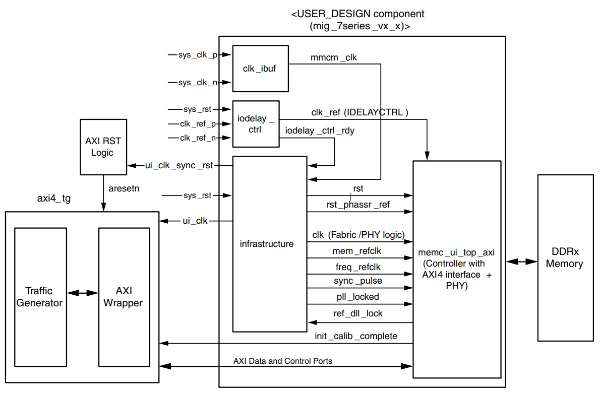
The example design uses a traffic generator to simulate the host PC reading/writing data from/to the MIG core. While useful, Xilinx’s implementation is slightly obfuscated, so we will replace it with our own VIP traffic generator moving forward.
The MIG’s reset scheme is as follows:
Raise the
sys_rst portHIGH, since we defined it as active HIGH.By doing this, the
ui_sync_rstport also goes HIGH.This port is passed into an inverter (the LUT1 in the schematic).
A LOW signal is sent from
aresetn_reg(also known asaresetn), which resets all AXI components (including both the traffic generator and MIG).
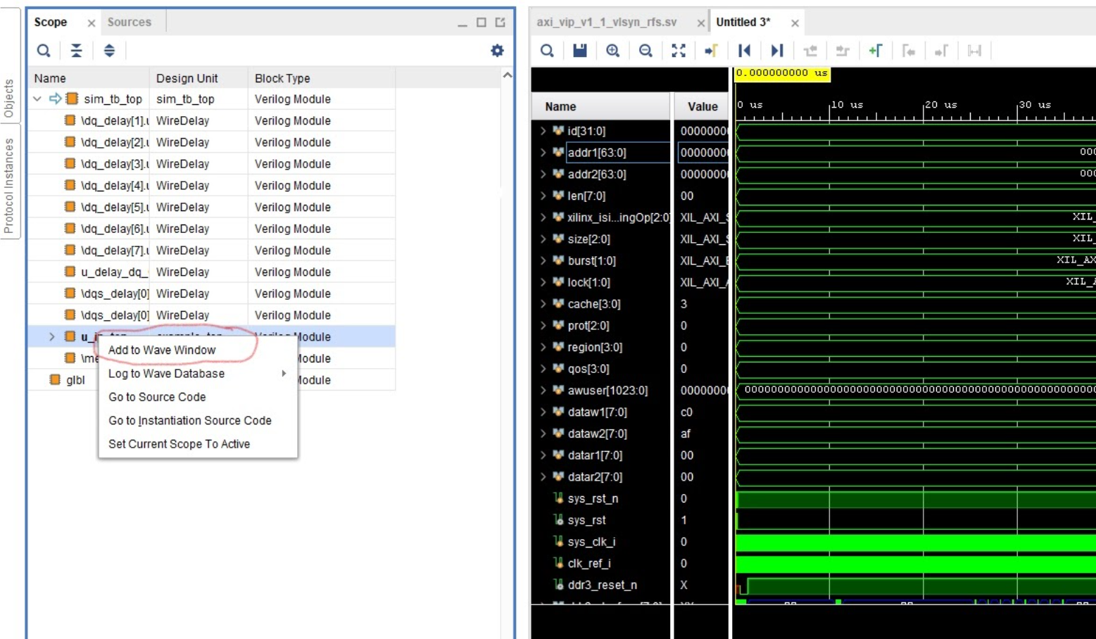
We can observe this behavior by running a Behavioral Simulation in Vivado. Make sure to add
the correct AXI signals by clicking the Scope heading, right clicking on the u_ip_top module
and selecting Add to Wave Window. This will allow us to see the AXI read and write transactions.
Note
If you need a refresher on the AXI protocol or interpreting the simulation’s waveforms, check here.
Since the MIG needs time to calibrate and set up, no AXI reads/writes will occur until after the init_calib_complete
pin goes HIGH after 100us.
After running the MIG’s Behavioral Simulation, you should observe that the AXI Address Width is 27 bits and the AXI Data Width is 32 bits, whfich is expected.
Tip
To find AXI parameter values such as Address or Data Width and Base Address, look for the comment AXI4 Shim parameters in the u_mig_7series_4_mig module.
1.3. Simulating Read/Writes with AXI VIP
Note
All further examples are implemented using a Kintex-7 FPGA. However, the most pertinent portions apply to all other FPGAs (e.g., the VIP implementation can also be used in the VC707’s provided testbench).
As mentioned before, Xilinx’s implementation of their Traffic Generator is difficult to break down into understandable chunks. Luckily, Xilinx also provides an alternative — the AXI Verification IP (or AXI VIP), which can simulate an AXI master, slave, or pass-through device. You can find more information about this IP through its product guide (PG267), but for our purposes, we will instead manually instantiate the IP using the example design.
Open the example_top module and comment out the entire traffic generator instantiation. It will have
a comment above it stating The traffic generation module instantiated below drives traffic (patterns)
on the application interface of the memory controller.
Make sure to also disable all the traffic generator-related source files: mig_7series_v4_2_axi4_tg.v,
mig_7series_v4_2_axi4_wrapper.v, mig_7series_v4_2cmd_prbs_gen_axi.v, mig_7series_v4_2_data_gen_chk.v,
and mig_7series_v4_2_tg.v. In the abstracted block diagram (BD) above, we are essentially replacing the
entire axi4_tg module.
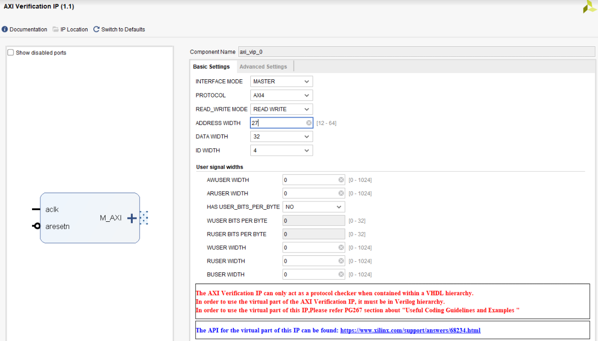
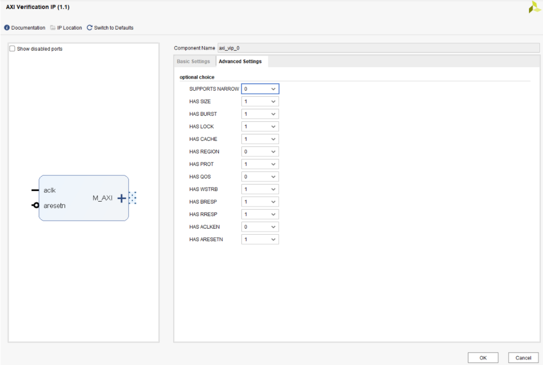
Using the IP Catalog, customize the AXI VIP as such:
Open the top module of the AXI VIP (axi_vip_0), copy all input/output signals (listed underneath
module axi_vip_0), and paste these signals back into the example_top.v file in place of the
commented-out TG instantiation.
Important
If you want to download the top file instead, go here. Just be sure to rename example_top_axi.v to example_top.v!
//***************************************************************************
// The traffic generation module instantiated below drives traffic (patterns)
// on the application interface of the memory controller
//***************************************************************************
   always @(posedge clk) begin
   aresetn <= ~rst;
   end

//INSTANTIATE AXI VIP INSTEAD OF TRAFFIC GENERATOR

axi_vip_0 u_axi_vip_0 (
   .aclk(clk),
   .aresetn(aresetn),
   .m_axi_awid(s_axi_awid),
   .m_axi_awaddr(s_axi_awaddr),
   .m_axi_awlen(s_axi_awlen),
   .m_axi_awsize(s_axi_awsize),
   .m_axi_awburst(s_axi_awburst),
   .m_axi_awlock(s_axi_awlock),
   .m_axi_awcache(s_axi_awcache),
   .m_axi_awprot(s_axi_awprot),
   .m_axi_awvalid(s_axi_awvalid),
   .m_axi_awready(s_axi_awready),
   .m_axi_wdata(s_axi_wdata),
   .m_axi_wstrb(s_axi_wstrb),
   .m_axi_wlast(s_axi_wlast),
   .m_axi_wvalid(s_axi_wvalid),
   .m_axi_wready(s_axi_wready),
   .m_axi_bid(s_axi_bid),
   .m_axi_bresp(s_axi_bresp),
   .m_axi_bvalid(s_axi_bvalid),
   .m_axi_bready(s_axi_bready),
   .m_axi_arid(s_axi_arid),
   .m_axi_araddr(s_axi_araddr),
   .m_axi_arlen(s_axi_arlen),
   .m_axi_arsize(s_axi_arsize),
   .m_axi_arburst(s_axi_arburst),
   .m_axi_arlock(s_axi_arlock),
   .m_axi_arcache(s_axi_arcache),
   .m_axi_arprot(s_axi_arprot),
   .m_axi_arvalid(s_axi_arvalid),
   .m_axi_arready(s_axi_arready),
   .m_axi_rid(s_axi_rid),
   .m_axi_rdata(s_axi_rdata),
   .m_axi_rresp(s_axi_rresp),
   .m_axi_rlast(s_axi_rlast),
   .m_axi_rvalid(s_axi_rvalid),
   .m_axi_rready(s_axi_rready)
);

// COMMENT THIS PART OUT BELOW
mig_7series_v4_2_axi4_tg #(
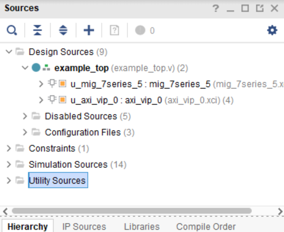
If synthesis completes, the AXI VIP has been successfully instantiated into the design in place of the traffic generator. The file hierarchy should be like this:
We can now add our AXI VIP testbench into the simulation top file sim_tb_top. We will use
SystemVerilog to implement this testbench, so right click on the file, select Set File Type,
and change the simulation language to SystemVerilog.
The objective of this testbench is to write some data to the DDR memory and read back from the
addresses we specified to compare the data. To achieve this, first initialize the AXI VIP in
sim_tb_top like so:
import axi_vip_pkg::*; //import packages for the AXI VIP
import axi_vip_0_pkg::*;

module sim_tb_top;

//declare AXI agent as master
axi_vip_0_mst_t      agent;

//define parameters for AXI VIP
axi_transaction            wr_trans1, wr_trans2; //two AXI write transactions
axi_transaction            rd_trans1, rd_trans2; //two AXI read transactions
xil_axi_uint               id =0; //default
xil_axi_ulong              addr1 =32'h0000, addr2 = 32'h0004; //define two test addresses
xil_axi_len_t              len =0; //only one burst
xil_axi_size_t             size =xil_axi_size_t'(xil_clog2((32)/8)); //default, maximum of 4 words per transaction (4 bytes for 32 bit AXI bus)
xil_axi_burst_t            burst =XIL_AXI_BURST_TYPE_INCR; //default,incremental burst type
xil_axi_lock_t             lock = XIL_AXI_ALOCK_NOLOCK; //default
xil_axi_cache_t            cache =3; //default
xil_axi_prot_t             prot =0; //default
xil_axi_region_t           region =0; //default
xil_axi_qos_t              qos =0; //default
xil_axi_data_beat [255:0]  wuser =0; //default
xil_axi_data_beat          awuser =0; //default
bit [7:0]                  dataw1 = 8'hC0, dataw2 = 8'hAF; //define two data words for AXI writes
bit[7:0]                   datar1, datar2; //if successful, these should match dataw1 and dataw2
Then, we perform two writes into DDR, one to address 0x0000 of data 0xC0 and the other to address 0x0004 of data 0xAF, and two reads from the same addresses, through:
//***************************************************************************
// Reporting the test case status
// Status reporting logic exists both in simulation test bench (sim_tb_top)
// and sim.do file for ModelSim. Any update in simulation run time or time out
// in this file need to be updated in sim.do file as well.
//***************************************************************************
initial
begin : Logging

   fork
      begin : calibration_done
         wait (init_calib_complete); //wait until init_calib_complete is done
         $display("Calibration Done");

         #100000; //100 ns delay

         agent = new("master vip agent",u_ip_top.u_axi_vip_0.inst.IF); //pass correct IF path
         agent.start_master(); //start master agent

         //begin write transactions to address 1 and address 2
         wr_trans1 = agent.wr_driver.create_transaction("single_write"); //initialize first transaction
         wr_trans1.set_write_cmd(addr1,burst,id,len,size); //declare address 1, as well as burst length and size
         wr_trans1.set_prot(prot); //set all other default parameters
         wr_trans1.set_lock(lock);
         wr_trans1.set_cache(cache);
         wr_trans1.set_region(region);
         wr_trans1.set_qos(qos);
         wr_trans1.set_data_block(dataw1); //put data1 on the AXI data bus
         agent.wr_driver.send(wr_trans1); //send write transaction

         #100000; //100 ns delay

         wr_trans2 = agent.wr_driver.create_transaction("single_write"); //initialize second transaction
         wr_trans2.set_write_cmd(addr2,burst,id,len,size); //declare address 2, as well as burst length and size
         wr_trans2.set_prot(prot); //set all other default parameters
         wr_trans2.set_lock(lock);
         wr_trans2.set_cache(cache);
         wr_trans2.set_region(region);
         wr_trans2.set_qos(qos);
         wr_trans2.set_data_block(dataw2); //put data2 on the AXI data bus
         agent.wr_driver.send(wr_trans2); //send write transaction

         #100000; //100 ns delay

         //begin read transaction to address 1 and address 2
         rd_trans1 = agent.rd_driver.create_transaction("single_read"); //initialize read transaction
         rd_trans1.set_read_cmd(addr1,burst,id,len,size); //set the correct parameters
         rd_trans1.set_prot(prot);
         rd_trans1.set_lock(lock);
         rd_trans1.set_cache(cache);
         rd_trans1.set_region(region);
         rd_trans1.set_qos(qos);
         rd_trans1.set_driver_return_item_policy(XIL_AXI_PAYLOAD_RETURN); //default, set driver return policy
         agent.rd_driver.send(rd_trans1); //send read transaction
         agent.rd_driver.wait_rsp(rd_trans1); //wait for response signal
         datar1 = rd_trans1.get_data_block(); //obtain read data

         #100000; //100 ns delay

         rd_trans2 = agent.rd_driver.create_transaction("single_read"); //initialize read transaction
         rd_trans2.set_read_cmd(addr2,burst,id,len,size); //set correct parameters
         rd_trans2.set_prot(prot);
         rd_trans2.set_lock(lock);
         rd_trans2.set_cache(cache);
         rd_trans2.set_region(region);
         rd_trans2.set_qos(qos);
         rd_trans2.set_driver_return_item_policy(XIL_AXI_PAYLOAD_RETURN); //default, set driver return policy
         agent.rd_driver.send(rd_trans2); //send read transaction
         agent.rd_driver.wait_rsp(rd_trans2); //wait for response signal
         datar2 = rd_trans2.get_data_block(); //obtain read data

         #100000; //100 ns delay
         if (datar1 == dataw1 && datar2 == dataw2) begin //test successful if this condition is true
            $display("TEST PASSED");
         end
         else begin
            $display("TEST FAILED: DATA ERROR");
         end
         disable calib_not_done;
          $finish;
      end
We can now run our Behavioral Simulation, but make sure to add the AXI signals by opening the Scope
menu, right clicking on the ui_top file, and selecting Add to Wave Window.
During the simulation, init_calib_complete will go HIGH after about 100us, after which the
reads and writes will begin. sys_reset will be held HIGH for the first 200ns, causing the
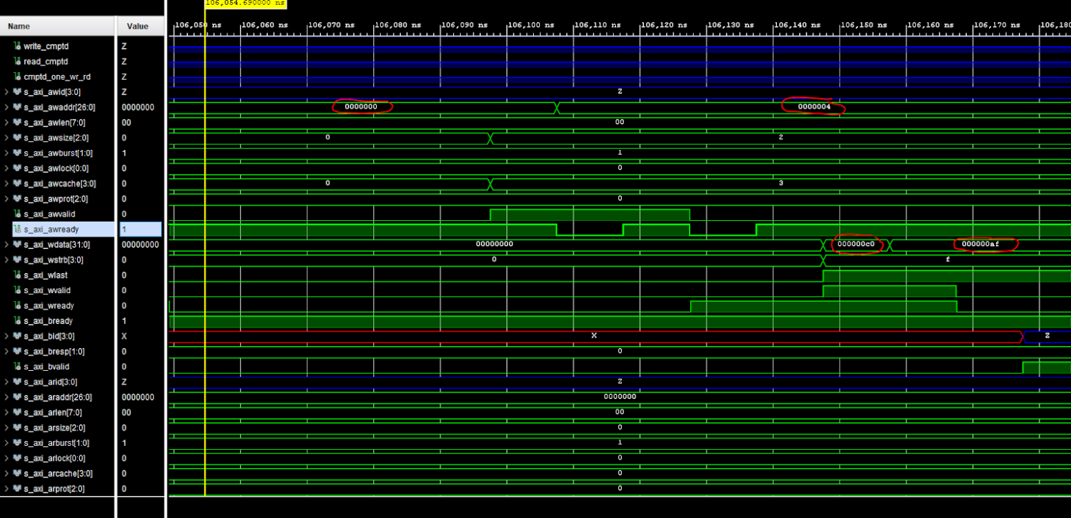
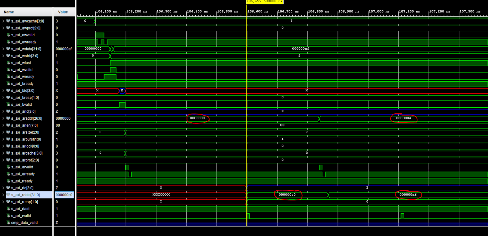
other resets to initiate and begin calibration. Here is what a successful simulation will look like:
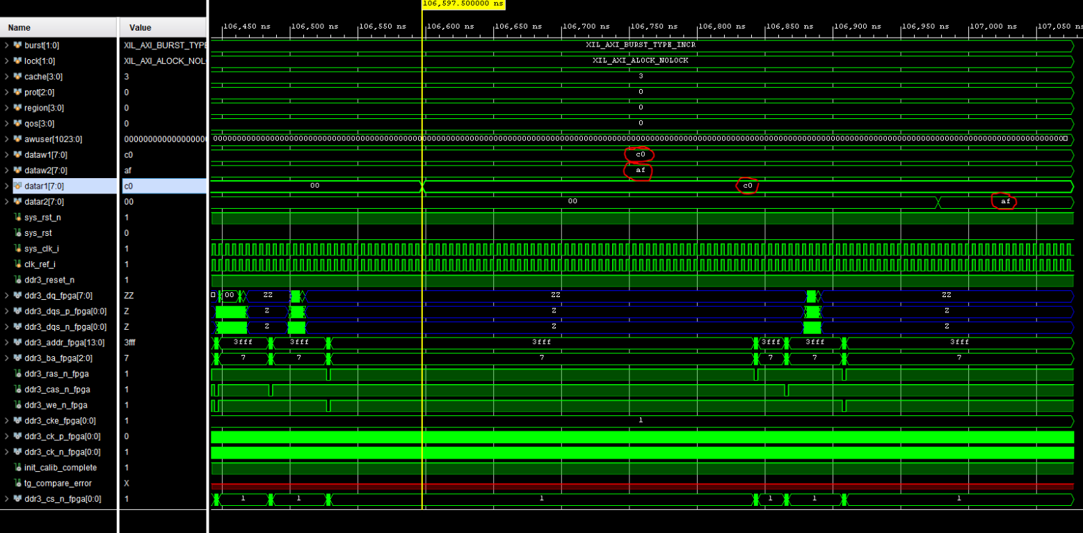
As we can see, the two bytes that were read from memory (c0 and af from datar1 and datar2, respectively)
matched the two bytes that were initially written to those memory addresses (dataw1 and dataw2). If your
simulation matches this, good job! The simulation was a success.
1.4. Connecting the MIG to a Custom Design
Perhaps you wish to connect the generated MIG to any AXI master, not just the AXI VIP. Using the VIP as another example, using the IP Integrator (making a BD) makes this process very straightforward.
The
ui_clkmust be driving the AXI read/write transactions to the MIG (i.e., theaclkon the AXI VIP).The
ui_clk_sync_rstmust be driving thearesetnpin on the AXI master (sinceui_clk_sync_rstis active HIGH andaresetnis active LOW, we use a Processor System Reset IP for easy conversion)The
sys_clk_iis the 200 MHz input clock that we defined in our MIG customization (which is also tied to the reference clock).sys_rstis the active HIGH reset that we defined in our MIG customization; bringing this pin HIGH will trigger theui_clk_sync_rst, which will in turn trigger thearesetnpin on the AXI master.init_calib_completetells us when the MIG calibration is complete, so that we can being using the DDR memory (will take about 100us to go HIGH in simulation).Finally, the external DDR bus connects to the physical RAM on the emulation board (bus outputs need to be assigned correctly using a XDC constraints file).
1.5. Connecting the MIG to Two AXI Master VIPs using AXI SmartConnect
After connecting one AXI VIP to the MIG, naturally we should also test dual reads/writes from two AXI masters simultaneously by connecting two AXI VIPs to a singular MIG. Later, we will use this principle to replace the AXI masters with a PCIe core and a DUT, moving closer to a full emulation environment. To achieve this, we will use an AXI SmartConnect IP.
Error
Xilinx now recommends that all new AXI designs use the SmartConnect v1.0 core. It is not recommended to use the AXI Interconnect v2.1 core.
Note
You can read more about the SmartConnect IP here.
Beginning with our modified MIG example design with one AXI VIP, create a new block diagram (BD). Add a SmartConnect IP and customize it as shown:
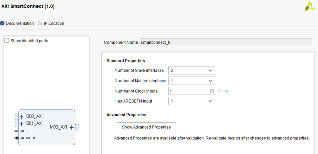
SmartConnect customization
Add two Master AXI VIP IPs to the BD and customize them:
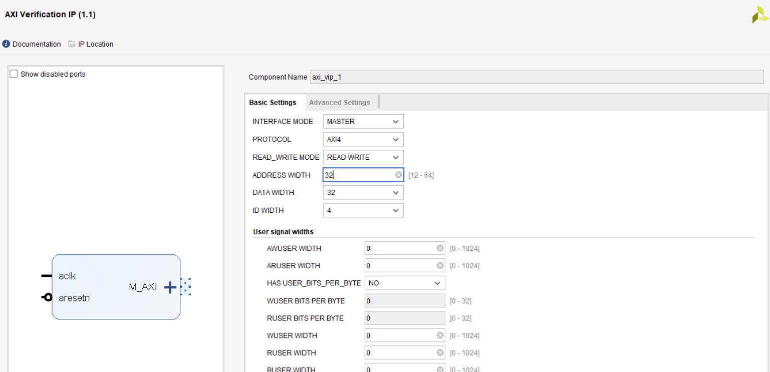
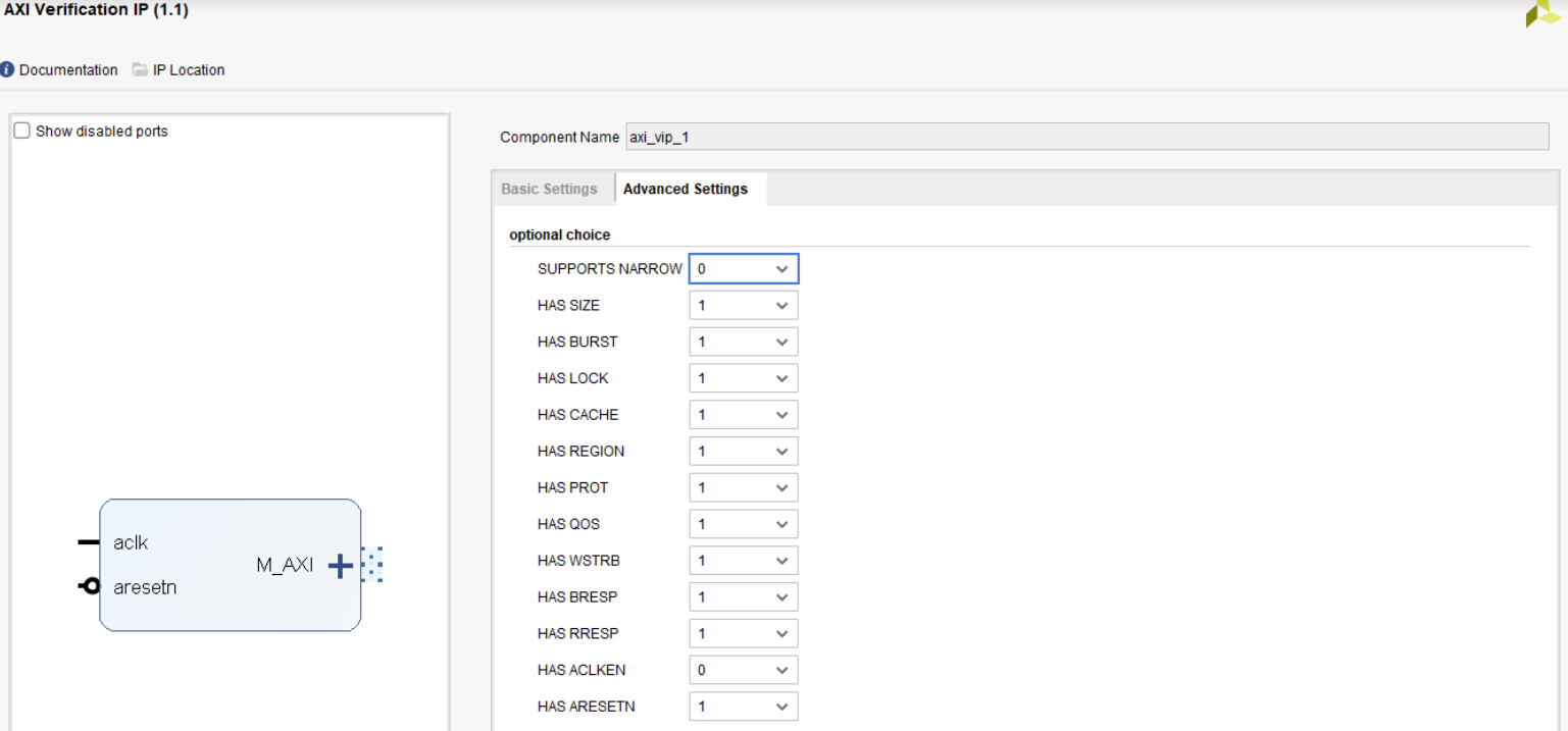
MIG AXI VIP customization
Connect them together in the BD (make aclk, aresetn, and M00_AXI external to instanitate them later):
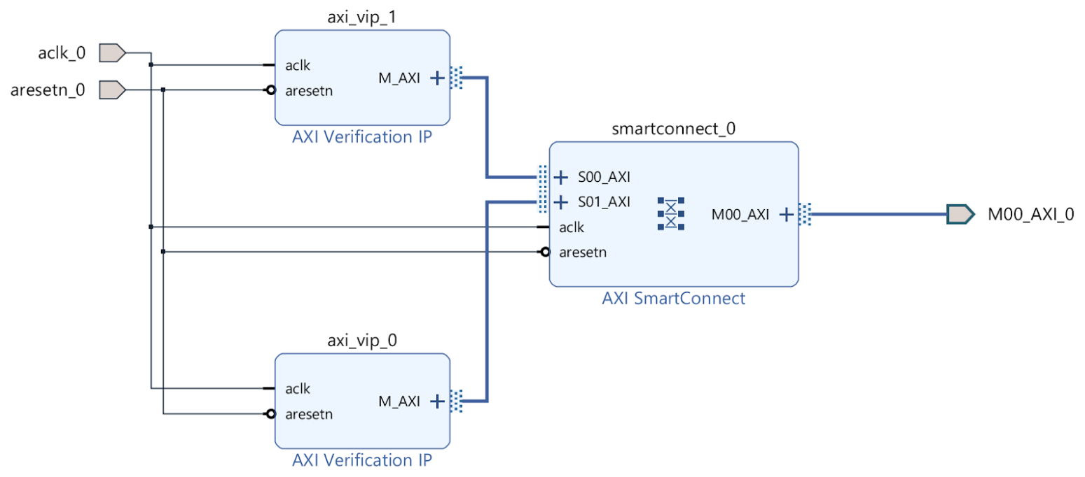
AXI VIP Block Diagram
If you try to Validate the BD now, a warning message about an unmapped slave will appear. To fix this, go to
the Address Editor tab and right click on the two AXI Master VIPs to map the M00_AXI_0 port to
Offset Address 0x0000_0000 for both AXI VIPs.
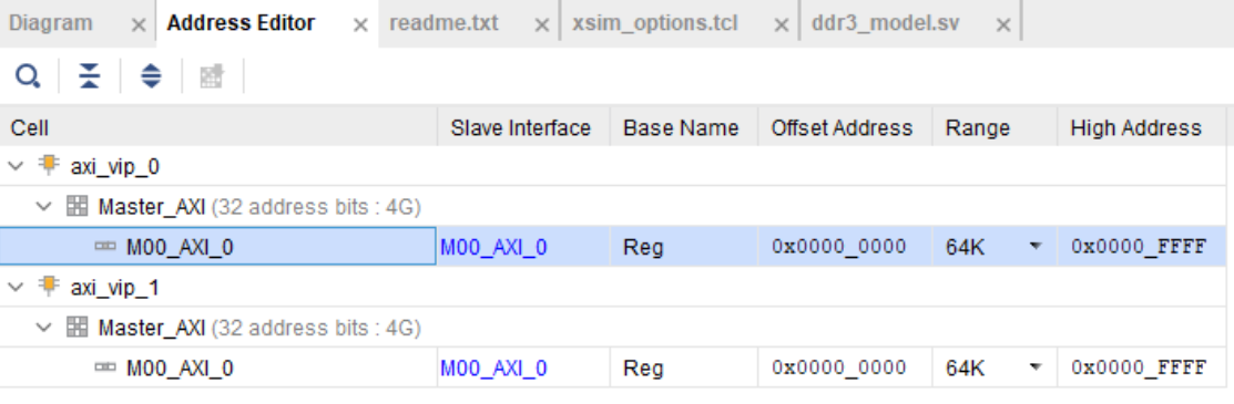
MIG AXI Address Editor
Make sure your design fully validates by right clicking the BD and selecting Validate Design.
Right click your BD in the Sources directory and Create a HDL Wrapper, which will generate the
RTL needed to instantiate our BD. When it is done generating, open the top file (default name is
similar to design_1_wrapper) and copy all inputs/outputs in the module.
Moving back to our MIG example_top file, remove the previous example instantiation of the AXI VIP
and insert the new instantiation with the ports from design_1_wrapper. It will look like this:
//***************************************************************************
// The traffic generation module instantiated below drives traffic (patterns)
// on the application interface of the memory controller
//***************************************************************************
   always @(posedge clk) begin
   aresetn <= ~rst;
   end

//INSTANTIATE Block Diagram with 2 AXI VIPs and an AXI Interconenct

design_1_wrapper u_axi_vip_interconnect_bd (

   //.M00_AXI_arid(s_axi_arid), //no port on AXI Smartconnect
   .M00_AXI_0_araddr(s_axi_araddr),
   .M00_AXI_0_arburst(s_axi_arburst),
   .M00_AXI_0_arcache(s_axi_arcache),
   .M00_AXI_0_arlen(s_axi_arlen),
   .M00_AXI_0_arlock(s_axi_arlock),
   .M00_AXI_0_arprot(s_axi_arprot),
   //.M00_AXI_0_arqos(s_axi_arqos), //no port on AXI Smartconnect
   .M00_AXI_0_arready(s_axi_arready),
   .M00_AXI_0_arsize(s_axi_arsize),
   .M00_AXI_0_arvalid(s_axi_arvalid),
   //.M00_AXI_awid(s_axi_awid), //no port on AXI Smartconnect
   .M00_AXI_0_awaddr(s_axi_awaddr),
   .M00_AXI_0_awburst(s_axi_awburst),
   .M00_AXI_0_awcache(s_axi_awcache),
   .M00_AXI_0_awlen(s_axi_awlen),
   .M00_AXI_0_awlock(s_axi_awlock),
   .M00_AXI_0_awprot(s_axi_awprot),
   //.M00_AXI_0_awqos(s_axi_awqos), //no port on AXI Smartconnect
   .M00_AXI_0_awready(s_axi_awready),
   .M00_AXI_0_awsize(s_axi_awsize),
   .M00_AXI_0_awvalid(s_axi_awvalid),
   //.M00_AXI_0_bid(s_axi_bid), //no port on AXI Smartconnect
   .M00_AXI_0_bready(s_axi_bready),
   .M00_AXI_0_bresp(s_axi_bresp),
   .M00_AXI_0_bvalid(s_axi_bvalid),
   .M00_AXI_0_rdata(s_axi_rdata),
   //.M00_AXI_0_rid(s_axi_rid), //no port on AXI Smartconnect
   .M00_AXI_0_rlast(s_axi_rlast),
   .M00_AXI_0_rready(s_axi_rready),
   .M00_AXI_0_rresp(s_axi_rresp),
   .M00_AXI_0_rvalid(s_axi_rvalid),
   .M00_AXI_0_wdata(s_axi_wdata),
   .M00_AXI_0_wlast(s_axi_wlast),
   .M00_AXI_0_wready(s_axi_wready),
   .M00_AXI_0_wstrb(s_axi_wstrb),
   .M00_AXI_0_wvalid(s_axi_wvalid),
   .aclk_0(clk),
   .aresetn_0(aresetn)
);

// COMMENT OUT THIS PART BELOW
mig_7series_v4_2_axi4_tg #(
Now we can run synthesis to verify that the top file compiles. There may be a small syntax error, which we can ignore.
Now that we have successfully instantiated our new design, our two AXI Masters should be able to perform read/write requests to the MIG through the AXI SmartConnect IP. We can verify this through a behavioral simulation that performs two simultaneous write/read requests to two different addresses.
Important
The simulation top file can be found here. Just be sure to rename example_top_2axi.v to example_top.v!
Note
This testbench will only work if you named your BD instantiation as u_axi_vip_interconnect_bd and left the component names of the AXI VIPs as default.
As before, make sure to instantiate the two AXI VIPs and their ports within the example testbench:
import axi_vip_pkg::*; //import packages for the AXI VIP
import design_1_axi_vip_0_0_pkg::*;
import design_1_axi_vip_0_1_pkg::*;

module sim_tb_top;

//declare AXI agent as master
design_1_axi_vip_0_0_mst_t      agent0;
design_1_axi_vip_0_1_mst_t      agent1;

//define parameters for AXI VIP
axi_transaction            wr_trans1, wr_trans2; //two AXI write transactions
axi_transaction            rd_trans1, rd_trans2; //two AXI read transactions
xil_axi_uint               id =0; //default
xil_axi_ulong              addr1 =32'h0000, addr2 = 32'h0004; //define two test addresses
xil_axi_len_t              len =0; //only one burst
xil_axi_size_t             size =xil_axi_size_t'(xil_clog2((32)/8)); //default, maximum of 4 words per transaction (4 bytes for 32 bit AXI bus)
xil_axi_burst_t            burst =XIL_AXI_BURST_TYPE_INCR; //default,incremental burst type
xil_axi_lock_t             lock = XIL_AXI_ALOCK_NOLOCK; //default
xil_axi_cache_t            cache =3; //default
xil_axi_prot_t             prot =0; //default
xil_axi_region_t           region =0; //default
xil_axi_qos_t              qos =0; //default
xil_axi_data_beat [255:0]  wuser =0; //default
xil_axi_data_beat          awuser =0; //default
bit [7:0]                  dataw1 = 8'hC0, dataw2 = 8'hAF; //define two data words for AXI writes
bit[7:0]                   datar1, datar2; //if successful, these should match dataw1 and dataw2
Then we set up two write and read requests using both AXI VIPs to two specified addresses, using the same procedure as our last testbench with one AXI VIP.
//***************************************************************************
// Reporting the test case status
// Status reporting logic exists both in simulation test bench (sim_tb_top)
// and sim.do file for ModelSim. Any update in simulation run time or time out
// in this file need to be updated in sim.do file as well.
//***************************************************************************
initial
begin : Logging

   fork
      begin : calibration_done
         wait (init_calib_complete); //wait until init_calib_complete is done
         $display("Calibration Done");

         #100000; //100 ns delay

         agent0 = new("master vip agent",u_ip_top.u_axi_vip_interconnect_bd.design_1_i.axi_vip_0.inst.IF); //pass correct IF path
         agent0.start_master(); //start master agent
         agent1 = new("master vip agent",u_ip_top.u_axi_vip_interconnect_bd.design_1_i.axi_vip_1.inst.IF); //pass correct IF path
         agent1.start_master(); //start master agent

         //write using AXI VIP 1
         wr_trans1 = agent1.wr_driver.create_transaction("single_write"); //initialize first transaction
         wr_trans1.set_write_cmd(addr1,burst,id,len,size); //declare address 1, as well as burst length and size
         wr_trans1.set_prot(prot); //set all other default parameters
         wr_trans1.set_lock(lock);
         wr_trans1.set_cache(cache);
         wr_trans1.set_region(region);
         wr_trans1.set_qos(qos);
         wr_trans1.set_data_block(dataw1); //put data1 on the AXI data bus
         agent1.wr_driver.send(wr_trans1); //send write transaction

         //write using AXI VIP 0
         wr_trans2 = agent0.wr_driver.create_transaction("single_write"); //initialize second transaction
         wr_trans2.set_write_cmd(addr2,burst,id,len,size); //declare address 2, as well as burst length and size
         wr_trans2.set_prot(prot); //set all other default parameters
         wr_trans2.set_lock(lock);
         wr_trans2.set_cache(cache);
         wr_trans2.set_region(region);
         wr_trans2.set_qos(qos);
         wr_trans2.set_data_block(dataw2); //put data2 on the AXI data bus
         agent0.wr_driver.send(wr_trans2); //send write transaction

         #100000; //100 ns delay

         //read using AXI VIP 0
         rd_trans1 = agent0.rd_driver.create_transaction("single_read"); //initialize read transaction
         rd_trans1.set_read_cmd(addr1,burst,id,len,size); //set the correct parameters
         rd_trans1.set_prot(prot);
         rd_trans1.set_lock(lock);
         rd_trans1.set_cache(cache);
         rd_trans1.set_region(region);
         rd_trans1.set_qos(qos);
         rd_trans1.set_driver_return_item_policy(XIL_AXI_PAYLOAD_RETURN); //default, set driver return policy
         agent0.rd_driver.send(rd_trans1); //send read transaction
         agent0.rd_driver.wait_rsp(rd_trans1); //wait for response signal
         datar1 = rd_trans1.get_data_block(); //obtain read data

         //read using AXI VIP 1
         rd_trans2 = agent1.rd_driver.create_transaction("single_read"); //initialize read transaction
         rd_trans2.set_read_cmd(addr2,burst,id,len,size); //set correct parameters
         rd_trans2.set_prot(prot);
         rd_trans2.set_lock(lock);
         rd_trans2.set_cache(cache);
         rd_trans2.set_region(region);
         rd_trans2.set_qos(qos);
         rd_trans2.set_driver_return_item_policy(XIL_AXI_PAYLOAD_RETURN); //default, set driver return policy
         agent1.rd_driver.send(rd_trans2); //send read transaction
         agent1.rd_driver.wait_rsp(rd_trans2); //wait for response signal
         datar2 = rd_trans2.get_data_block(); //obtain read data

         #1000000; //1000 ns delay

         if (datar1 == dataw1 && datar2==dataw2) begin //test successful if this condition is true
            $display("TEST PASSED");
         end
         else begin
            $display("TEST FAILED: DATA ERROR");
         end
         disable calib_not_done;
          $finish;
      end
We can observe the simulation’s intended behavior by running a Behavioral Simulation.
Here we can see two AXI Write transactions — one writing data C0 to address 0x0000 and one writing data AF to address 0x0004.
We can also observe two AXI Read transactions, one from address 0x0000 reading data C0 and one from address 0x0004 reading data AF.
If the TCL console prints a Test Passed message, congratulations! The test worked and you have successfully implemented two AXI VIPs with a MIG.
sim_tb_top.mem_rnk[0].gen_mem[0].u_comp_ddr3.data_task: at time 107027064.0 ps INFO: READ @ DQS= bank = 0 row = 0000 col = 00000006 data = 00
sim_tb_top.mem_rnk[0].gen_mem[0].u_comp_ddr3.data_task: at time 107028314.0 ps INFO: READ @ DQS= bank = 0 row = 0000 col = 00000007 data = 00
sim_tb_top.mem_rnk[0].gen_mem[0].u_comp_ddr3.cmd_task: at time 107048314.0 ps INFO: Precharge bank   0

TEST PASSED
Executing Axi4 End of Simulation checks
Executing Axi4 End of Simulation checks
$finish called at time : 108227500 ps : File "..."