2. AXI MM to PCIe IP Overview
The AXI Memory Mapped to PCI Express IP is a useful core that is compatible with only some FPGAs, offering a different implementation than that offered by the 7 Series Integrated Block for PCIe IP. More information can be found in the IP’s documentation (PG055).
2.1. Customizing the IP
Create a new block diagram (BD) and use the IP catalog to add a new IP to the BD - in this case, the “AXI Memory Mapped to PCIe” core. We can customize it by double clicking it.
Important
Unless mentioned otherwise, leave all values default.
In the PCIE:Basics tab, set the Reference Clock frequency to 100 MHz.
Make sure we are customizing the device as an Endpoint.
Depending on the application, in the PCIE: Link Config tab, change the Land Width. Most boards support at least X4, although newer boards will support X8. In addition, select the highest possible Link Speed for maximum performance.
Again, depending on the application, you may change the Vendor ID and Class Code to something else. For example, if you plan to use this IP in conjunction with a soft CPU like MicroBlaze, you will change the Class Code to 0x060400 accordingly. If not, leave the entire tab default.
In the PCIE:BARs tab, set BAR 0 at a size of 64 kB at offset address 0x00000000 and BAR 1 at size 64 kB at address 0x40000000.
Every other tab can be left default.
2.2. Simulating the Example Design
After customizing, right click the IP block and open the IP Example Design.
The Example Design consists of the AXI MM to PCIe IP block connected to both a Block RAM (BRAM) Controller through the PCIe’s AXI Master port and a Root Complex simulation on the PCIe’s physical serial ports. Essentially, the example design simulates a host PC generating and sending traffic into the FPGA through the PCIe interface. The AXI MM to PCIe IP processes the incoming traffic and writes into BRAM using the AXI protocol.
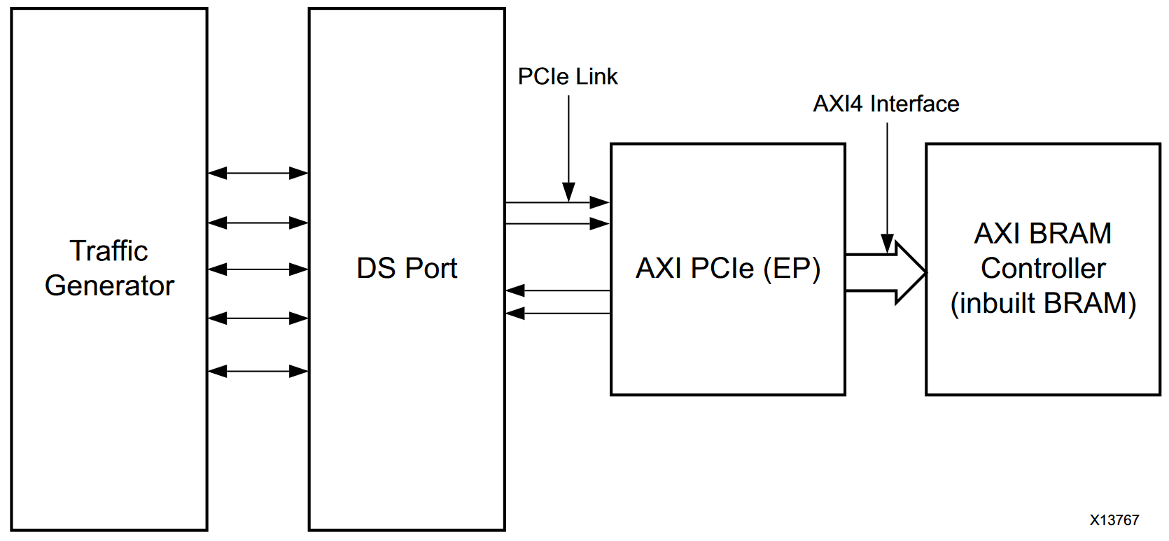
Abstracted PCIe Example Design BD
Note
If you need a refresher on the PCIe protocol, check here.
Like the MIG design, the PCIe example design must first spend 175 us calibrating and initializing its serial ports. It then performs a simple write to address 0x10 in BRAM and subsequently reads it back, verifying that the read data matches what was written.
The PCIe serial ports take much longer to initialize than the MIG’s. If you run a Behavioral Simulation,
do not be surprised if nothing happens at first. The simulation may stall after returning the message
Built simulation snapshot board_behav. Since, by default, the simulation only runs for less
than 1 us, simply use the command run -all in the TCL console to allow the serial lines to start
toggling and the simulation to fully complete.
After around 30 minutes to 1 hour, you should receive a message in the console stating that the testbench has timed out. If the simulation is successful, the TCL console will also show that the test passed.
Note
The simulation will only work for one registered BAR in the IP. If you customized your IP to have multiple BARs, like we did, you will receive a message that the second BAR was disabled for this simulation.
[   207869316] : TSK_PARSE_FRAME on Receive
[   209749220] : Transmitting TLPs to Memory 32 Space BAR 0
[   209767229] : TSK_PARSE_FRAME on Transmit
[   209805308] : TSK_PARSE_FRAME on Transmit
[   212125269] : TSK_PARSE_FRAME on Receive
[   213797220] : Test PASSED --- Write Data: 01020304 successfully received
[   213837220] : Finished transmission of PCI-Express TLPs
Test Completed Successfully
$finish called at time 213837220 ps : File "..."
2.3. Example IP Block Diagram
After running Block and Connection Automation, the AXI MM to PCIe IP example BD will look similar to this:
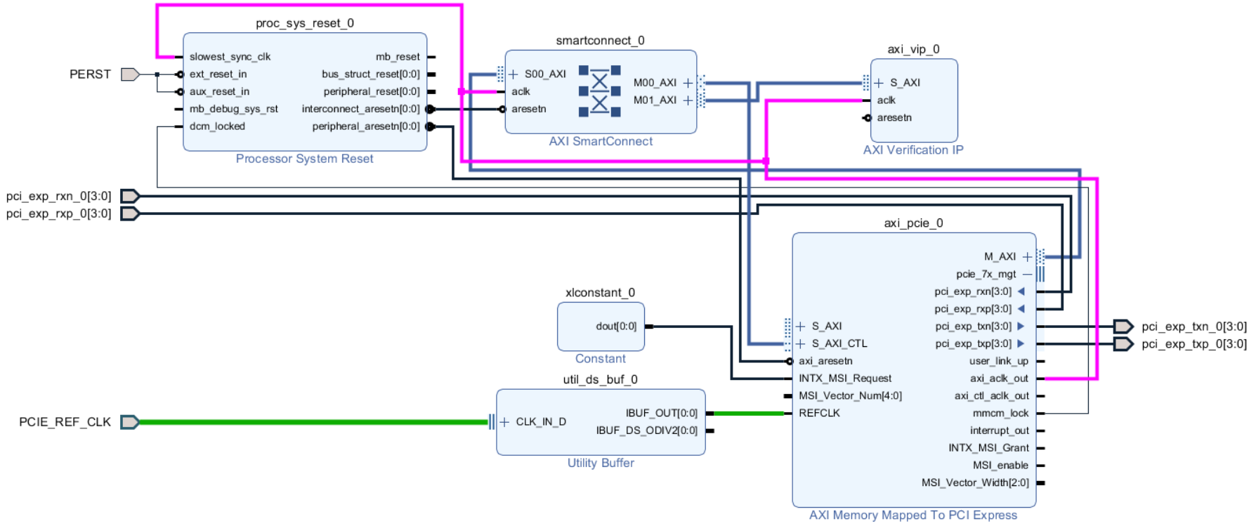
PCIe Block Diagram
The PCIe Reference Clock (
REFCLK) at 100 MHz will go through an IBUFDSGTE Utility Buffer.The physical
PERST(PCIe reset) pin is connected to a Processor System Reset IP, with the output going into theaxi_aresetnport.The
INTX_MSI_Requestport is connected to a Constant block tied active LOW (0) to prevent unwanted MSI interrupts.The
M_AXIport feeds into an AXI SmartConnect, where our AXI Slave devices are connected. The other AXI slave at this moment is a basic AXI Verification IP (VIP).The
S_AXI_CTLport can be used as an AXI Slave port to perform reads and writes to the PCIe Configuration Space.The
axi_aclk_outport outputs a clock frequency of 125 MHz, which is the frequency that the AXI MM to PCIe Core operates at. It is currently clocking the SmartConnect and AXI VIP, which is typically not recommended (should use a Clocking Wizard for all other peripherals).The
pcie_7x_mgtports are all external ports that connect to the physical PCIe port. They control the serial transactions between the root complex and PCIe endpoint.
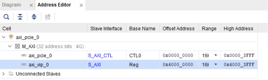
To ensure that our customized BARs are accurately reflected in our AXI Slave devices, we must assign
the correct addresses using the Address Editor. Map the S_AXI_CTL slave to address 0x00000000 and
the AXI VIP slave to address 0x40000000.
2.4. Replacing the BRAM with DDR MIG in Example Design
Create a new BD and insert an AXI SmartConnect with one AXI Master input, one AXI Slave output, 64-bit Data Width, and two clock inputs. This SmartConnect will resolve the different clock domains that the PCIe IP and MIG run at.
Once the SmartConnect wrapper has been added to the project, open the IP catalog, and select the MIG 7 Series IP, customizing it like this.
After the MIG has been generated, we will instanitate the MIG and SmartConnect into the example
design top file. Open xilinx_axi_pcie_ep.v and remove the instantiation of the BRAM Controller,
replacing it with instantiations of both the MIG and SmartConnect.
Important
If you want to download the top file instead, go here.
//INSTANTIATE MIG CORE
mig_7series_5 u_mig_7series_5(

// Memory interface ports
    .ddr3_addr                      (ddr3_addr),
    .ddr3_ba                        (ddr3_ba),
    .ddr3_cas_n                     (ddr3_cas_n),
    .ddr3_ck_n                      (ddr3_ck_n),
    .ddr3_ck_p                      (ddr3_ck_p),
    .ddr3_cke                       (ddr3_cke),
    .ddr3_ras_n                     (ddr3_ras_n),
    .ddr3_we_n                      (ddr3_we_n),
    .ddr3_dq                        (ddr3_dq),
    .ddr3_dqs_n                     (ddr3_dqs_n),
    .ddr3_dqs_p                     (ddr3_dqs_p),
    .ddr3_reset_n                   (ddr3_reset_n),
    .init_calib_complete            (init_calib_complete),
    .ddr3_cs_n                      (ddr3_cs_n),
    .ddr3_dm                        (ddr3_dm),
    .ddr3_odt                       (ddr3_odt),

// Application interface ports
    .ui_clk                         (clk),
    .ui_clk_sync_rst                (rst),
    .mmcm_locked                    (mmcm_locked),
    .aresetn                        (aresetn),

    .app_sr_req(app_sr_req),
    .app_ref_req(app_ref_req),  //HAD TO ADD THESE MANUALLY
    .app_zq_req(app_zq_req),

    .app_sr_active                  (app_sr_active),
    .app_ref_ack                    (app_ref_ack),
    .app_zq_ack                     (app_zq_ack),

// Slave Interface Write Address Ports
    .s_axi_awid                     (s_axi_awid),
    .s_axi_awaddr                   (s_axi_awaddr),
    .s_axi_awlen                    (s_axi_awlen),
    .s_axi_awsize                   (s_axi_awsize),
    .s_axi_awburst                  (s_axi_awburst),
    .s_axi_awlock                   (s_axi_awlock),
    .s_axi_awcache                  (s_axi_awcache),
    .s_axi_awprot                   (s_axi_awprot),
    .s_axi_awqos                    (4'h0),
    .s_axi_awvalid                  (s_axi_awvalid),
    .s_axi_awready                  (s_axi_awready),

// Slave Interface Write Data Ports
    .s_axi_wdata                    (s_axi_wdata),
    .s_axi_wstrb                    (s_axi_wstrb),
    .s_axi_wlast                    (s_axi_wlast),
    .s_axi_wvalid                   (s_axi_wvalid),
    .s_axi_wready                   (s_axi_wready),

// Slave Interface Write Response Ports
    .s_axi_bid                      (s_axi_bid),
    .s_axi_bresp                    (s_axi_bresp),
    .s_axi_bvalid                   (s_axi_bvalid),
    .s_axi_bready                   (s_axi_bready),

// Slave Interface Read Address Ports
    .s_axi_arid                     (s_axi_arid),
    .s_axi_araddr                   (s_axi_araddr),
    .s_axi_arlen                    (s_axi_arlen),
    .s_axi_arsize                   (s_axi_arsize),
    .s_axi_arburst                  (s_axi_arburst),
    .s_axi_arlock                   (s_axi_arlock),
    .s_axi_arcache                  (s_axi_arcache),
    .s_axi_arprot                   (s_axi_arprot),
    .s_axi_arqos                    (4'h0),
    .s_axi_arvalid                  (s_axi_arvalid),
    .s_axi_arready                  (s_axi_arready),

// Slave Interface Read Data Ports
    .s_axi_rid                      (s_axi_rid),
    .s_axi_rdata                    (s_axi_rdata),
    .s_axi_rresp                    (s_axi_rresp),
    .s_axi_rlast                    (s_axi_rlast),
    .s_axi_rvalid                   (s_axi_rvalid),
    .s_axi_rready                   (s_axi_rready),

// System Clock Ports
    .sys_clk_i                       (sys_clk_i),
    .device_temp                     (device_temp),

    `ifdef SKIP_CALIB
    .calib_tap_req                    (calib_tap_req),
    .calib_tap_load                   (calib_tap_load),
    .calib_tap_addr                   (calib_tap_addr),
    .calib_tap_val                    (calib_tap_val),
    .calib_tap_load_done              (calib_tap_load_done),
    `endif

    .sys_rst                        (sys_rst)
);

assign s_axi_awid = 4'h0; //tie off unneeded ports to 0
assign s_axi_arid = 4'h0;
assign app_sr_req = 1'h0;
assign app_ref_req = 1'h0;
assign app_zq_req = 1'h0;

always @(posedge clk) begin
    aresetn <= ~rst;
end

//INSTANTIATE AXI SMARTCONNECT MODULE
design_1_wrapper u_axi_smartconnect(

    //Master ports going into MIG
    .M00_AXI_0_araddr(s_axi_araddr),
    .M00_AXI_0_arburst(s_axi_arburst),
    .M00_AXI_0_arcache(s_axi_arcache),
    .M00_AXI_0_arlen(s_axi_arlen),
    .M00_AXI_0_arlock(s_axi_arlock),
    .M00_AXI_0_arprot(s_axi_arprot),
    //.M00_AXI_0_arqos(s_axi_arqos),
    .M00_AXI_0_arready(s_axi_arready),
    .M00_AXI_0_arsize(s_axi_arsize),
    .M00_AXI_0_arvalid(s_axi_arvalid),
    .M00_AXI_0_awaddr(s_axi_awaddr),
    .M00_AXI_0_awburst(s_axi_awburst),
    .M00_AXI_0_awcache(s_axi_awcache),
    .M00_AXI_0_awlen(s_axi_awlen),
    .M00_AXI_0_awlock(s_axi_awlock),
    .M00_AXI_0_awprot(s_axi_awprot),
    //.M00_AXI_0_awqos(s_axi_awqos),
    .M00_AXI_0_awready(s_axi_awready),
    .M00_AXI_0_awsize(s_axi_awsize),
    .M00_AXI_0_awvalid(s_axi_awvalid),
    .M00_AXI_0_bready(s_axi_bready),
    .M00_AXI_0_bresp(s_axi_bresp),
    .M00_AXI_0_bvalid(s_axi_bvalid),
    .M00_AXI_0_rdata(s_axi_rdata),
    .M00_AXI_0_rlast(s_axi_rlast),
    .M00_AXI_0_rready(s_axi_rready),
    .M00_AXI_0_rresp(s_axi_rresp),
    .M00_AXI_0_rvalid(s_axi_rvalid),
    .M00_AXI_0_wdata(s_axi_wdata),
    .M00_AXI_0_wlast(s_axi_wlast),
    .M00_AXI_0_wready(s_axi_wready),
    .M00_AXI_0_wstrb(s_axi_wstrb),
    .M00_AXI_0_wvalid(s_axi_wvalid),

    //Slave ports coming from the PCIE
    .S00_AXI_0_araddr(m_axi_araddr),
    .S00_AXI_0_arburst(m_axi_arburst),
    .S00_AXI_0_arcache(m_axi_arcache),
    .S00_AXI_0_arlen(m_axi_arlen),
    .S00_AXI_0_arlock(m_axi_arlock),
    .S00_AXI_0_arprot(m_axi_arprot),
    //.S00_AXI_0_arqos(m_axi_arqos),
    .S00_AXI_0_arready(m_axi_arready),
    .S00_AXI_0_arsize(m_axi_arsize),
    .S00_AXI_0_arvalid(m_axi_arvalid),
    .S00_AXI_0_awaddr(m_axi_awaddr),
    .S00_AXI_0_awburst(m_axi_awburst),
    .S00_AXI_0_awcache(m_axi_awcache),
    .S00_AXI_0_awlen(m_axi_awlen),
    .S00_AXI_0_awlock(m_axi_awlock),
    .S00_AXI_0_awprot(m_axi_awprot),
    //.S00_AXI_0_awqos(m_axi_awqos),
    .S00_AXI_0_awready(m_axi_awready),
    .S00_AXI_0_awsize(m_axi_awsize),
    .S00_AXI_0_awvalid(m_axi_awvalid),
    .S00_AXI_0_bready(m_axi_bready),
    .S00_AXI_0_bresp(m_axi_bresp),
    .S00_AXI_0_bvalid(m_axi_bvalid),
    .S00_AXI_0_rdata(m_axi_rdata),
    .S00_AXI_0_rlast(m_axi_rlast),
    .S00_AXI_0_rready(m_axi_rready),
    .S00_AXI_0_rresp(m_axi_rresp),
    .S00_AXI_0_rvalid(m_axi_rvalid),
    .S00_AXI_0_wdata(m_axi_wdata),
    .S00_AXI_0_wlast(m_axi_wlast),
    .S00_AXI_0_wready(m_axi_wready),
    .S00_AXI_0_wstrb(m_axi_wstrb),
    .S00_AXI_0_wvalid(m_axi_wvalid),

    //Clocks and Resets
    .aclk1_0(clk), //MIG clock (100MHz)
    .aclk_0(axi_aclk_out), //PCIE clock (125MHz)
    .aresetn_0(aresetn) //use MIG reset signal
);
We will also add in the necessary MIG ports and parameters that was present in the MIG example design.
//INSERT PARAMETERS FOR MIG

//***************************************************************************
// Traffic Gen related parameters
//***************************************************************************
parameter BEGIN_ADDRESS         = 32'h00000000,
parameter END_ADDRESS           = 32'h00ffffff,
parameter PRBS_EADDR_MASK_POS   = 32'hff000000,
parameter ENFORCE_RD_WR         = 0,
parameter ENFORCE_RD_WR_CMD     = 8'h11,
parameter ENFORCE_RD_WR_PATTERN = 3'b000,
parameter C_EN_WRAP_TRANS       = 0,
parameter C_AXI_NBURST_TEST     = 0,

//***************************************************************************
// The following parameters refer to width of various ports
//***************************************************************************
parameter CK_WIDTH              = 1, // # of CK/CK# outputs to memory.
parameter nCS_PER_RANK          = 1, // # of unique CS outputs per rank for phy
parameter CKE_WIDTH             = 1, // # of CKE outputs to memory.
parameter DM_WIDTH              = 1, // # of DM (data mask)
parameter ODT_WIDTH             = 1, // # of ODT outputs to memory.
parameter BANK_WIDTH            = 3, // # of memory Bank Address bits.
parameter COL_WIDTH             = 10, // # of memory Column Address bits.
parameter CS_WIDTH              = 1, // # of unique CS outputs to memory.
parameter DQ_WIDTH              = 8, // # of DQ (data)
parameter DQS_WIDTH             = 1,
parameter DQS_CNT_WIDTH         = 1, // = ceil(log2(DQS_WIDTH))
parameter DRAM_WIDTH            = 8, // # of DQ per DQS
parameter ECC                   = "OFF",
parameter ECC_TEST              = "OFF",
parameter nBANK_MACHS           = 4,
parameter RANKS                 = 1, // # of Ranks.
parameter ROW_WIDTH             = 14, // # of memory Row Address bits.
parameter ADDR_WIDTH            = 28, // # = RANK_WIDTH + BANK_WIDTH + ROW_WIDTH + COL_WIDTH;
                                        // Chip Select is always tied to low for single rank devices

//***************************************************************************
// The following parameters are mode register settings
//***************************************************************************
parameter BURST_MODE            = "8",// DDR3 SDRAM:
                                    // Burst Length (Mode Register 0).
                                    // # = "8", "4", "OTF".

//***************************************************************************
// The following parameters are multiplier and divisor factors for PLLE2.
// Based on the selected design frequency these parameters vary.
//***************************************************************************
parameter CLKIN_PERIOD          = 5000, // Input Clock Period
parameter CLKFBOUT_MULT         = 4,// write PLL VCO multiplier
parameter DIVCLK_DIVIDE         = 1, // write PLL VCO divisor
parameter CLKOUT0_PHASE         = 315.0,// Phase for PLL output clock (CLKOUT0)
parameter CLKOUT0_DIVIDE        = 1, // VCO output divisor for PLL output clock (CLKOUT0)
parameter CLKOUT1_DIVIDE        = 2,// VCO output divisor for PLL output clock (CLKOUT1)
parameter CLKOUT2_DIVIDE        = 32, // VCO output divisor for PLL output clock (CLKOUT2)
parameter CLKOUT3_DIVIDE        = 8,// VCO output divisor for PLL output clock (CLKOUT3)
parameter MMCM_VCO              = 800,// Max Freq (MHz) of MMCM VCO
parameter MMCM_MULT_F           = 8, // write MMCM VCO multiplier
parameter MMCM_DIVCLK_DIVIDE    = 1,// write MMCM VCO divisor

//***************************************************************************
// Simulation parameters
//***************************************************************************
parameter SIMULATION            = "FALSE",
                                    // Should be TRUE during design simulations and
                                    // FALSE during implementations

//***************************************************************************
// IODELAY and PHY related parameters
//***************************************************************************


parameter TCQ_MIG                   = 0.1, //100 ps for MIG


parameter DRAM_TYPE             = "DDR3",
//***************************************************************************
// System clock frequency parameters
//***************************************************************************
parameter nCK_PER_CLK           = 4, // # of memory CKs per fabric CLK

//***************************************************************************
// AXI4 Shim parameters
//***************************************************************************
parameter C_S_AXI_ID_WIDTH              = 4, // Width of all master and slave ID signals. # = >= 1.
parameter C_S_AXI_ADDR_WIDTH            = 27,// Width of S_AXI_AWADDR, S_AXI_ARADDR, M_AXI_AWADDR and M_AXI_ARADDR for all SI/MI slots. # = 32.
parameter C_S_AXI_DATA_WIDTH            = 32, // Width of WDATA and RDATA on SI slot. Must be <= APP_DATA_WIDTH. # = 32, 64, 128, 256.
parameter C_S_AXI_SUPPORTS_NARROW_BURST = 0, // Indicates whether to instatiate upsizer. Range: 0, 1

//***************************************************************************
// Debug parameters
//***************************************************************************
parameter DEBUG_PORT            = "OFF",// # = "ON" Enable debug signals/controls. "OFF" Disable debug signals/controls.
parameter RST_ACT_LOW           = 0// =1 for active low reset, =0 for active high.

) (

output  [3:0]    pci_exp_txp,
output  [3:0]    pci_exp_txn,
input   [3:0]    pci_exp_rxp,
input   [3:0]    pci_exp_rxn,

input            sys_clk_p,
input            sys_clk_n,
input            sys_rst_n, //ACTIVE LOW

//INSERT INPUTS/OUTPUTS FOR MIG
// Inouts

inout [7:0]                       ddr3_dq,
inout [0:0]                       ddr3_dqs_n,
inout [0:0]                       ddr3_dqs_p,

// Outputs
output [13:0]                     ddr3_addr,
output [2:0]                      ddr3_ba,
output                            ddr3_ras_n,
output                            ddr3_cas_n,
output                            ddr3_we_n,
output                            ddr3_reset_n,
output [0:0]                      ddr3_ck_p,
output [0:0]                      ddr3_ck_n,
output [0:0]                      ddr3_cke,
output [0:0]                      ddr3_cs_n,
output [0:0]                      ddr3_dm,
output [0:0]                      ddr3_odt,

// Single-ended system clock
input                             sys_clk_i,
output                            tg_compare_error,
output                            init_calib_complete,

// System reset - Default polarity of sys_rst pin is Active Low.
// System reset polarity will change based on the option
// selected in GUI.
input                             sys_rst //Active HIGH

);

///////////////////////////

//INSERT FUNCTIONS FROM MIG TOP FILE

function integer clogb2 (input integer size);
    begin
    size = size - 1;
    for (clogb2=1; size>1; clogb2=clogb2+1)
        size = size >> 1;
    end
endfunction // clogb2

function integer STR_TO_INT;
    input [7:0] in;
    begin
    if(in == "8")
        STR_TO_INT = 8;
    else if(in == "4")
        STR_TO_INT = 4;
    else
        STR_TO_INT = 0;
    end
endfunction

//INSERT LOCALPARAMS FROM MIG TOP FILE

localparam DATA_WIDTH            = 8;
localparam RANK_WIDTH = clogb2(RANKS);
localparam PAYLOAD_WIDTH         = (ECC_TEST == "OFF") ? DATA_WIDTH : DQ_WIDTH;
localparam BURST_LENGTH          = STR_TO_INT(BURST_MODE);
localparam APP_DATA_WIDTH        = 2 * nCK_PER_CLK * PAYLOAD_WIDTH;
localparam APP_MASK_WIDTH        = APP_DATA_WIDTH / 8;
//***************************************************************************
// Traffic Gen related parameters (derived)
//***************************************************************************
localparam  TG_ADDR_WIDTH = ((CS_WIDTH == 1) ? 0 : RANK_WIDTH) + BANK_WIDTH + ROW_WIDTH + COL_WIDTH;
localparam MASK_SIZE             = DATA_WIDTH/8;
localparam DBG_WR_STS_WIDTH      = 40;
localparam DBG_RD_STS_WIDTH      = 40;

//INSERT MIG WIRE DECLARATIONS

wire                              clk;
wire                              rst;
wire                              mmcm_locked;
reg                               aresetn;
wire                              app_sr_active;
wire                              app_ref_ack;
wire                              app_zq_ack;
wire                              app_rd_data_valid;
wire [APP_DATA_WIDTH-1:0]         app_rd_data;
wire                              mem_pattern_init_done;
wire                              cmd_err;
wire                              data_msmatch_err;
wire                              write_err;
wire                              read_err;
wire                              test_cmptd;
wire                              write_cmptd;
wire                              read_cmptd;
wire                              cmptd_one_wr_rd;

//ADDITIONAL WIRES NEEDED TO ADD
wire         app_sr_req;

wire         app_ref_req;

wire         app_zq_req;

// Slave Interface Write Address Ports
wire [C_S_AXI_ID_WIDTH-1:0]       s_axi_awid;
wire [C_S_AXI_ADDR_WIDTH-1:0]     s_axi_awaddr;
wire [7:0]                        s_axi_awlen;
wire [2:0]                        s_axi_awsize;
wire [1:0]                        s_axi_awburst;
wire [0:0]                        s_axi_awlock;
wire [3:0]                        s_axi_awcache;
wire [2:0]                        s_axi_awprot;
wire                              s_axi_awvalid;
wire                              s_axi_awready;

// Slave Interface Write Data Ports
wire [C_S_AXI_DATA_WIDTH-1:0]     s_axi_wdata;
wire [(C_S_AXI_DATA_WIDTH/8)-1:0]   s_axi_wstrb;
wire                              s_axi_wlast;
wire                              s_axi_wvalid;
wire                              s_axi_wready;

// Slave Interface Write Response Ports
wire                              s_axi_bready;
wire [C_S_AXI_ID_WIDTH-1:0]       s_axi_bid;
wire [1:0]                        s_axi_bresp;
wire                              s_axi_bvalid;

// Slave Interface Read Address Ports
wire [C_S_AXI_ID_WIDTH-1:0]       s_axi_arid;
wire [C_S_AXI_ADDR_WIDTH-1:0]     s_axi_araddr;
wire [7:0]                        s_axi_arlen;
wire [2:0]                        s_axi_arsize;
wire [1:0]                        s_axi_arburst;
wire [0:0]                        s_axi_arlock;
wire [3:0]                        s_axi_arcache;
wire [2:0]                        s_axi_arprot;
wire                              s_axi_arvalid;
wire                              s_axi_arready;

// Slave Interface Read Data Ports
wire                              s_axi_rready;
wire [C_S_AXI_ID_WIDTH-1:0]       s_axi_rid;
wire [C_S_AXI_DATA_WIDTH-1:0]     s_axi_rdata;
wire [1:0]                        s_axi_rresp;
wire                              s_axi_rlast;
wire                              s_axi_rvalid;
wire                              cmp_data_valid;
wire [C_S_AXI_DATA_WIDTH-1:0]     cmp_data;     // Compare data
wire [C_S_AXI_DATA_WIDTH-1:0]     rdata_cmp;      // Read data
wire                              dbg_wr_sts_vld;
wire [DBG_WR_STS_WIDTH-1:0]       dbg_wr_sts;
wire                              dbg_rd_sts_vld;
wire [DBG_RD_STS_WIDTH-1:0]       dbg_rd_sts;
wire [11:0]                       device_temp;

`ifdef SKIP_CALIB // skip calibration wires
wire                          calib_tap_req;
reg                           calib_tap_load;
reg [6:0]                     calib_tap_addr;
reg [7:0]                     calib_tap_val;
reg                           calib_tap_load_done;
`endif
assign tg_compare_error = cmd_err | data_msmatch_err | write_err | read_err;
In addition, we need to tie some of the MIG input wires to ground, since the SmartConnect itself does not have every connection, as well as initialize the debug ports and calibration logic.
//INSERT REMAINING RTL FROM MIG TOP FILE
//*****************************************************************
// Default values are assigned to the debug inputs
//*****************************************************************
assign dbg_sel_pi_incdec       = 'b0;
assign dbg_sel_po_incdec       = 'b0;
assign dbg_pi_f_inc            = 'b0;
assign dbg_pi_f_dec            = 'b0;
assign dbg_po_f_inc            = 'b0;
assign dbg_po_f_dec            = 'b0;
assign dbg_po_f_stg23_sel      = 'b0;
assign po_win_tg_rst           = 'b0;
assign vio_tg_rst              = 'b0;

`ifdef SKIP_CALIB

//***************************************************************************
// Skip calib test logic
//***************************************************************************
reg[3*DQS_WIDTH-1:0]        po_coarse_tap;
reg[6*DQS_WIDTH-1:0]        po_stg3_taps;
reg[6*DQS_WIDTH-1:0]        po_stg2_taps;
reg[6*DQS_WIDTH-1:0]        pi_stg2_taps;
reg[5*DQS_WIDTH-1:0]        idelay_taps;
reg[11:0]                   cal_device_temp;

always @(posedge clk) begin
    // tap values from golden run (factory)
    po_coarse_tap   <= #TCQ_MIG 'h2;
    po_stg3_taps    <= #TCQ_MIG 'h0D;
    po_stg2_taps    <= #TCQ_MIG 'h1D;
    pi_stg2_taps    <= #TCQ_MIG 'h1E;
    idelay_taps     <= #TCQ_MIG 'h08;
    cal_device_temp <= #TCQ_MIG 'h000;
end

always @(posedge clk) begin
    if (rst)
    calib_tap_load <= #TCQ_MIG 1'b0;
    else if (calib_tap_req)
    calib_tap_load <= #TCQ_MIG 1'b1;
end

always @(posedge clk) begin
    if (rst) begin
    calib_tap_addr      <= #TCQ_MIG 'd0;
    calib_tap_val       <= #TCQ_MIG po_coarse_tap[3*calib_tap_addr[6:3]+:3]; //'d1;
    calib_tap_load_done <= #TCQ_MIG 1'b0;
    end else if (calib_tap_load) begin
    case (calib_tap_addr[2:0])
        3'b000: begin
        calib_tap_addr[2:0] <= #TCQ_MIG 3'b001;
        calib_tap_val       <= #TCQ_MIG po_stg3_taps[6*calib_tap_addr[6:3]+:6]; //'d19;
        end
        3'b001: begin
        calib_tap_addr[2:0] <= #TCQ_MIG 3'b010;
        calib_tap_val       <= #TCQ_MIG po_stg2_taps[6*calib_tap_addr[6:3]+:6]; //'d45;
        end

        3'b010: begin
        calib_tap_addr[2:0] <= #TCQ_MIG 3'b011;
        calib_tap_val       <= #TCQ_MIG pi_stg2_taps[6*calib_tap_addr[6:3]+:6]; //'d20;
        end

        3'b011: begin
        calib_tap_addr[2:0] <= #TCQ_MIG 3'b100;
        calib_tap_val       <= #TCQ_MIG idelay_taps[5*calib_tap_addr[6:3]+:5]; //'d1;
        end

        3'b100: begin
        if (calib_tap_addr[6:3] < DQS_WIDTH-1) begin
            calib_tap_addr[2:0] <= #TCQ_MIG 3'b000;
            calib_tap_val       <= #TCQ_MIG po_coarse_tap[3*(calib_tap_addr[6:3]+1)+:3]; //'d1;
            calib_tap_addr[6:3] <= #TCQ_MIG calib_tap_addr[6:3] + 1;
        end else begin
            calib_tap_addr[2:0] <= #TCQ_MIG 3'b110;
            calib_tap_val       <= #TCQ_MIG cal_device_temp[7:0];
            calib_tap_addr[6:3] <= #TCQ_MIG 4'b1111;
        end
        end

        3'b110: begin
            calib_tap_addr[2:0] <= #TCQ_MIG 3'b111;
            calib_tap_val       <= #TCQ_MIG {4'h0,cal_device_temp[11:8]};
            calib_tap_addr[6:3] <= #TCQ_MIG 4'b1111;
        end

        3'b111: begin
            calib_tap_load_done <= #TCQ_MIG 1'b1;
        end
    endcase
    end
end

//****************skip calib test logic end**********************************

`endif
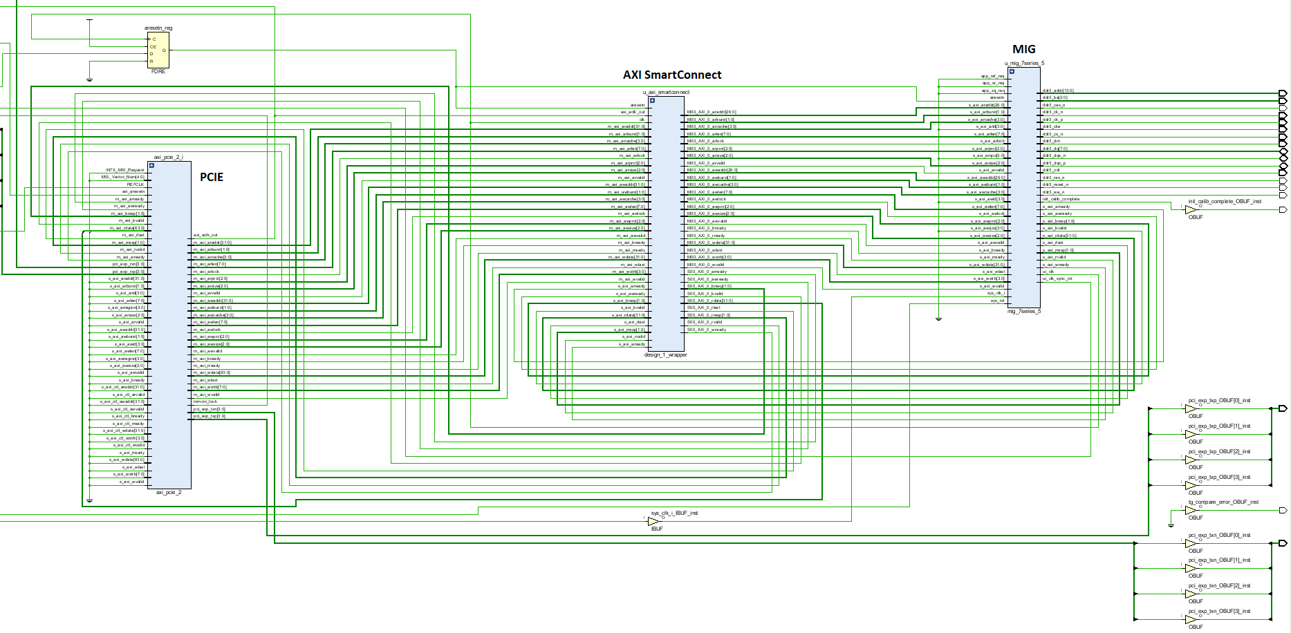
The complete PCIe and MIG schematic
2.5. Simulating the AXI MM PCIe MIG Example Design
After instantiating the MIG into the PCIe’s example design, we also need to copy over some modules from the MIG’s generated design for the PCIe MIG simulation to run properly. We need to import the relevant DDR3 Memory Model and Wire Delay modules.
Note
The MIG 7 Series IP Example Design will output these modules, so generate the design if you have not done so already.
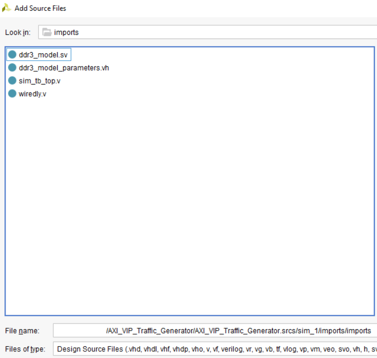
In the Source directory, select Add Sources, Add or Create Simulation Sources, and then point it to the modules in the MIG Example Design folder located in the user directory. On Windows (or Linux), navigate to the directory where your MIG project is saved.
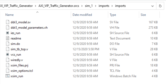
From there, locate the project’s imported directory. An example directory would be similar to <project name>\srcs\sim_1\imports\imports.
The directory should look like this:
Select the ddr3_model.sv, ddr3_model_parameters.vh, and wiredly.v files to add them
to the project.
Modify the simulation top file to properly instantiate these new modules, including
all MIG parameters. The example simulation top file can be found here. Make sure to rename axi_pcie_board.v to board.v!
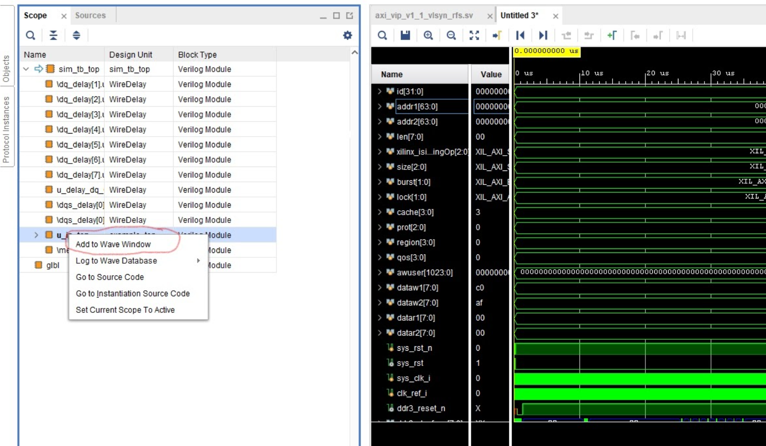
Run a Behavioral Simulation, making sure to add the propery AXI signals for the DUT in the
Scope Window (such as the u_ip_top module).
Important
Remember to run the command run -all in the TCL console to allow the simulation to fully complete!
The MIG will take about 120 us to fully calibrate. Afterwards, the
init_calib_completepin will go HIGH, outputting this message in the TCL console.
board.mem_rnk[0].gen_mem[0].u_comp_ddr3.cmd_task: at time 120768564.0 ps INFO: Refresh
board.mem_rnk[0].gen_mem[0].u_comp_ddr3.cmd_task: at time 122328564.0 ps INFO: Activate bank 0 row 0000
PHY_INIT: Write Calibration completed at 124203100.0 ps
board.mem_rnk[0].gen_mem[0].u_comp_ddr3.cmd_task: at time 125424564.0 ps INFO: Precharge All
board.mem_rnk[0].gen_mem[0].u_comp_ddr3.cmd_task: at time 125424564.0 ps INFO: Precharge bank 0
MIG Calibration Done
Around 200 us, the PCIe Endpoint will also fully calibrate. The simulated Root Port Complex will then begin to send Transaction Layer Packets (TLPs) to the PCIe Endpoint signaling for a read and a write to the DDR3 memory.
The Endpoint will then convert these TLPs to the correct AXI Memory Mapped read/write signals and send these through the SmartConnect into the MIG. Eventually, the MIG will receive these AXI requests on its AXI Slave port and subsequently perform the desired reads/writes to the simulated DDR3 memory.
If successful, the TCL console will output this message:
[187477264.0 ps] : TSK_PARSE_FRAME on Receive
[187781296.0 ps] : Test PASSED --- Write Data: 01020304 successfully received
[187821329.0 ps] : Finished transmission of PCI-Express TLPs
Test Completed Successfully
$finish called at time : 187821329 ps : File "..."
Like the original PCIe example design simulation, this test writes the data 0x01020304 to address 0x00000010. It then reads the data back from the same address, verifying that it is the same value. If your simulation looks like this, congratulations! You have successfully implemented a PCIe Endpoint with a MIG Controller.
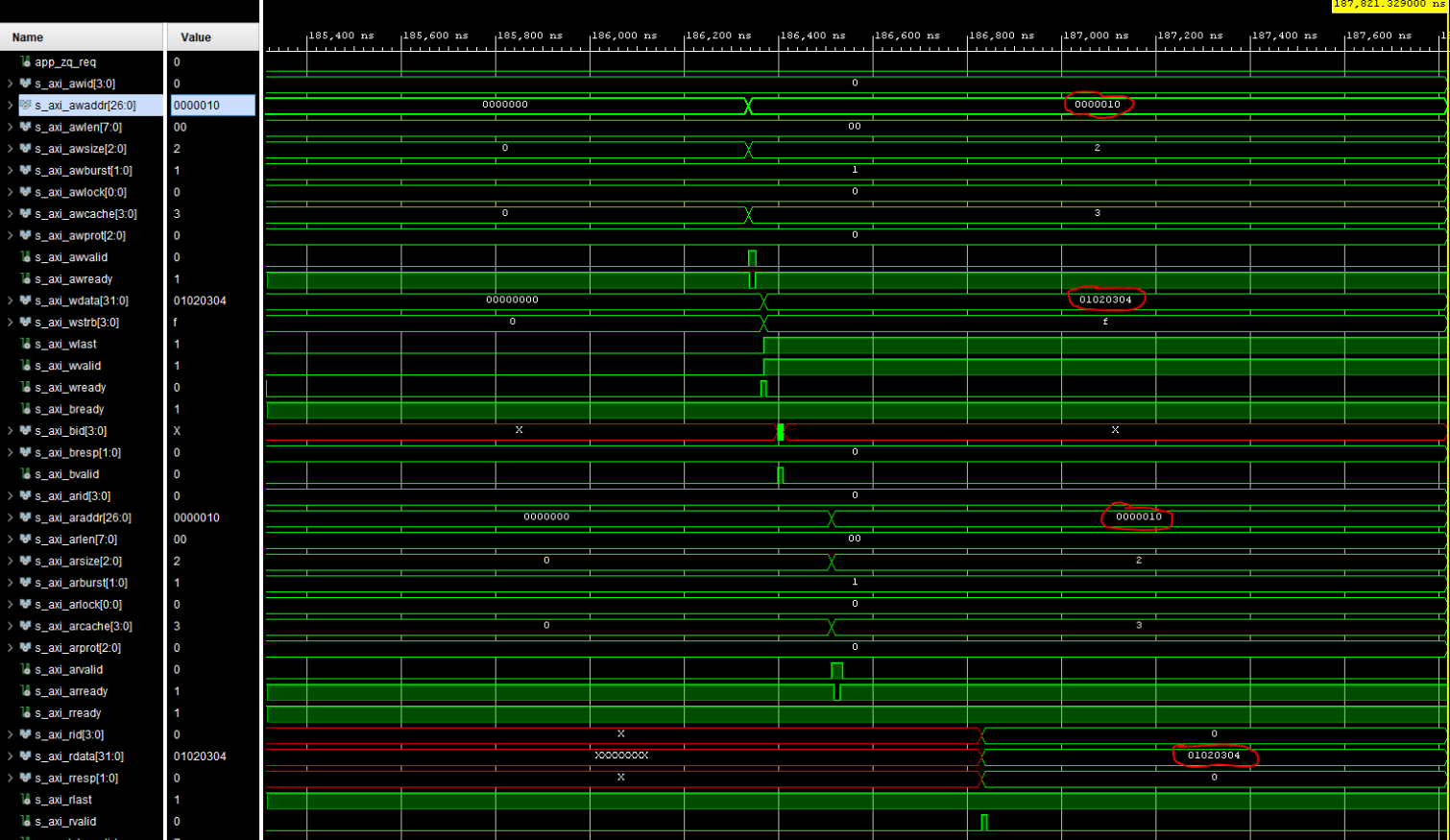
Successful PCIe Simulation