2. Building an Emulation Environment (without a Board)
Note
All pages are under construction as we work to finalize this project. Please be patient!
Important
This guide uses Vivado 2020.2, so while the software and IPs will change in the future, underlying principles will remain the same.
Create a new project and select your project device. For this article, we will assume that no pre-existing board files will be used, except for the MIG’s UCF constraint file. For example, we will use the Virtex-7 2000T FPGA for this design (similar to the HTG-700 development board from HTG which both has DDR3 SoDIMM memory and 8x Gen.3 PCIe) which at the moment does not have prepackaged board files in a standard Vivado installation. This design should also work with Vivado’s WebPACK version (eg. you can use the Kintex-7 XCKU025 which is compatible with all IPs), given you have access or are willing to write UCF and XDC constraints.
As such, we will not include any source files within this article, except our example AXI counter. We encourage you to step through and generate the design yourself, as parameters will vary between FPGAs. We will, however, give samples of our source code so that you can step through the process yourself.
Here is a companion video with the Virtex-7 2000T that can be used alongside this article for further clarification.
2.1. Project Start (Building the Block Diagram)
If you need a refresher on digital design and FPGAs, read this article first.
If this is your first Vivado project, make sure you download the Vivado Design Suite here. If you wish to follow this tutorial with a Virtex-7 or equivalent FPGA and have access to a license, use Vivado’s License Manager to install the license. Otherwise, download the WebPACK version for access to the Kintex-7 FPGAs.
Note
As of Vivado 2020.2, there is a bug where Vivado cannot create a project if there is a space in your Windows/Linux username. Be careful if you try to use this or earlier versions.
Create a new RTL project and choose your project device. For this article, we will choose the xc7v000tflg1925-2 FPGA. After the project initializes, create a new block diagram (also referred to as a BD).
In your new BD, generate a DMA/Bridge Subsystem for PCI Express IP using the plus sign at the top of the BD window. Each FPGA will require a different customization, but you can refer to our companion video for our example configuration. After the IP has been generated, right click the IP block and select Open IP Example Design…, allowing Vivado to generate and manage everything. A new example design project will automatically open.
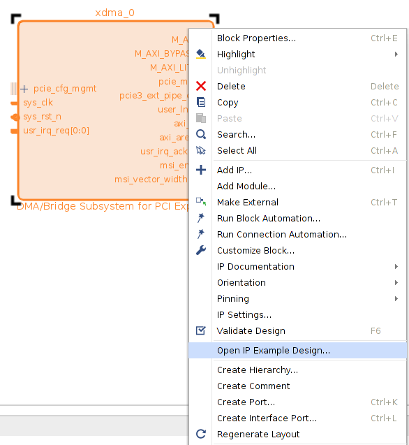
Opening the example design for XDMA IP
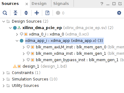
Source Directory of our new XDMA project
After the example XDMA project opens, create a new block design in this new project (you can close out of the first project, as we will not use it going forward). The current source directory should look similar to this:
In this BD, generate a AXI SmartConnect, which we will use to control each IP. You can read more about AXI and the
SmartConnect here. We generated our SmartConnect with 2 Master and 3 Slave interfaces,
2 Clock Inputs, and an ARESETN input. The PCIe Master has 3 BARs, so there are 3 slave interfaces. We also have 2 AXI masters
for both the DUT and MIG, and 2 Clocks for the PCIe and MIG. aclk_0 is the PCIe reference clock (in this case is 125 MHz) and must be
clocked seperately from the entire system. We will use the MIG’s clock for the rest of the design. Also generate a MIG 7 Series
IP for our onboard DDR3 memory. You can read more about the MIG here. For our MIG customization, refer
to our companion video as a guide, but make sure you have access to a UCF pin constraints file (examples can be found online).
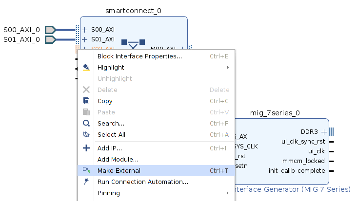
With both IPs in the BD generated, make the S00_AXI, S01_AXI, S02_AXI, aclk_0, and aresetn_0 ports of
smartconnect_0 and the SYS_CLK_0, sys_rst_0, DDR3_0, ui_clk_sync_rst_0, ui_clk_0, mmcm_locked_0,
and init_calib_complete_0 ports of mig_7series_0 external by right clicking each port and selecting Make External.
We are making these pins external to utilize them elsewhere in the design and to monitor them during simulation, so we will
instantiate these pins in Verilog later.
Making MIG and SmartConnect pins external
Double click on the S00_AXI_0, S01_AXI_0, and S02_AXI_0 pins to modify their parameters. S00_AXI_0 and S01_AXI_0 will
represent the two data signals from our DMA PCIe top module (DMA and bypass). You can read more about the DMA PCIe IP here.
As such, to properly connect both signals, S00 and S01 should be set to AXI4 and the ID Width for both S00 and S01 needs to be set to
4 (as the PCIe AXI data signals will throw an error when not set to 4 or unconnected). The AXI ID width determines how many IDs we can allocate
(2^4 = 16), which in turn determines how many transactions the AXI Master can track and reorder with the AXI transaction ID (side note - packet
reordering allows an AXI Master to correctly order transactions to ensure data integrity, akin to TCP networking). The ID width itself is determined
by the number of bits between cap_max_link_width - 1:0 (eg. X4 = C_M_AXI_ID_WIDTH-1 = 3:0 which is 4 bits). We will use an AXI data width of
64 bits and an address width of 32 bits.
The external S02 pin corresponds to the DUT. The parameters will depend based on which DUT is being tested. In our example, we will test an
AXI4Lite DUT, which only has a data width of 32 bits and an ID width of 0 (as there are no ID signals in the AXI4Lite protocol). Accordingly, we will
set the protocol of the S02 pin to AXI4Lite.